Mila
May 28,2026
364
Mila
May 28,2026
364
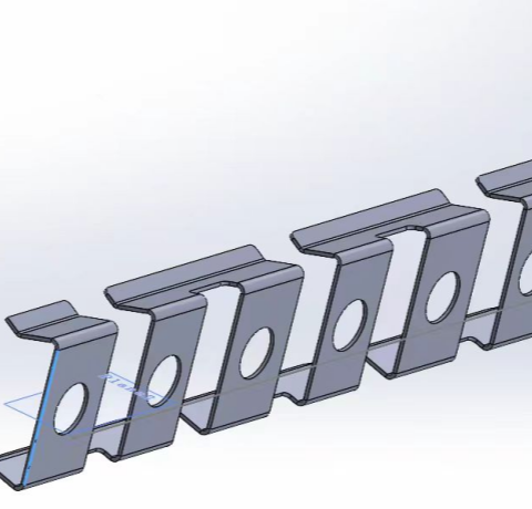
Sheet Metal Box Design Guide: 12 Common DFM Mistakes to Avoid
Sheet metal fabrication is widely used for enclosures, brackets, chassis, and industrial housings through processes such as cutting, bending, welding, and surface finishing. Although many designs look...
Mila
May 26,2026
1430
Complete Sheet Metal Box Design Guide for Electronic Enclosures
With the advantages of controllable cost, reliable strength, and efficient manufacturing, sheet metal enclosures are widely used in electronics, industrial control, telecommunications, medical equipme...
 Engineer
May 22,2026
780
Engineer
May 22,2026
780
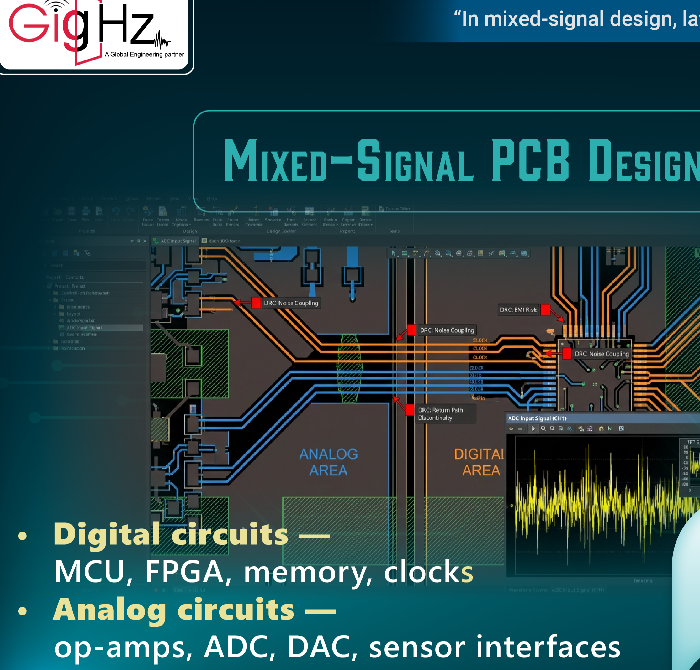
Mixed-Signal PCB Design: A Practical Engineering Guide
Mixed-Signal PCB Design: A Practical Engineering GuideMany PCB performance issues are not caused by firmware or components — they originate in the layout itself.When a mixed-signal board shows unstabl...
Mila
May 21,2026
2025
Decoupling Capacitor Placement Guidelines for High-Speed PCB Design
Many high-speed PCBs appear correct during schematic design, yet after fabrication, problems such as FPGA configuration failures, unstable DDR timing, ADC noise, EMC radiation issues, and excessive po...
Mila
May 18,2026
1866
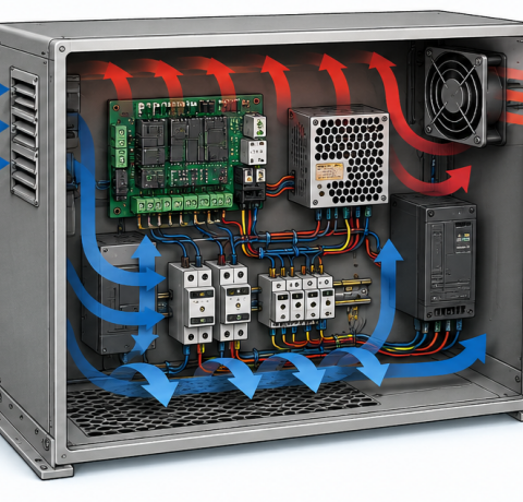
Electronic Enclosure Thermal Management: Cooling Design and Best Practices
Enclosure thermal management is critical for preventing overheating, condensation, and premature electronic component failure. A well-designed enclosure cooling system helps maintain stable operating ...
Mila
May 14,2026
2017
EMI Shielded Enclosure Design Guide: Principles, Materials, and Best Practices
EMI (Electromagnetic Interference) has become a major challenge in modern electronic systems. In many projects, EMI-related issues do not appear during early development, but instead emerge during EMC...
Mila
May 11,2026
2227
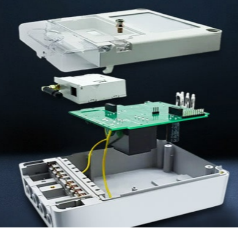
PCB Enclosure Design Guide: Materials, IP Ratings, and Structural Best Practices
In electronic product development, enclosure design is often underestimated. Even when the PCB functions correctly, poor enclosure design can still lead to overheating, assembly interference, insuffic...
Mila
May 07,2026
1493
Basic PCB Design: Complete PCB Design Guidelines for Beginners
PCB is the core carrier of modern electronic devices. From wearable products to servers and automotive electronics, reliable PCB design is essential to system performance and stability. Many beginners...
Mila
Apr 30,2026
1109
DCDC Power PCB Layout Guidelines: Reduce Noise, Improve Stability, and Pass EMC
In DCDC power design, the circuit defines the function, but PCB layout determines success or failure. Even with correct component selection and accurate calculations, issues such as audible noise, ove...
Mila
Apr 24,2026
2306
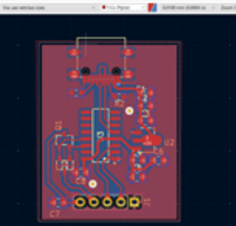
PCB Layout Design Guide: Practical Guidelines and Best Practices for Reliable PCB Design
PCB design is the complete process of electronic system development, including schematic design, component selection, PCB layout, rule checking, and manufacturing output. PCB layout, however, is the c...
PCBWay
Apr 22,2026
1870
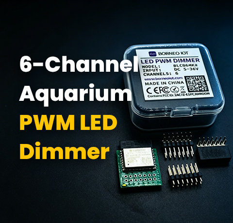
PCBWayer Bazaar NewArrival Product - 6-Channel Wi-Fi PWM LED Dimmer
Link:6-Channel Wi-Fi PWM LED DimmerBuce (BLC06) is an OSHWA-certified open-source, 6-channel all-in-one Wi-Fi LED PWM dimmer module designed for high-end aquatic lighting systems.FeaturesThe Buce modu...
Mila
Apr 22,2026
1908
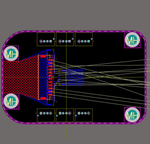
PCB Schematic Design Guide: From Concept to Production-Ready PCB
In many hardware projects, schematic design is often underestimated. Engineers move into PCB layout before fully defining circuit logic, signal flow, and design constraints, which can lead to multiple...
Mila
Apr 13,2026
1033
Why 90% of EMC Issues Come from Poor Grounding in PCB Design
During hardware development, failing EMC tests is a common issue. Many engineers try fixes such as adding shielding enclosures, replacing chips, or increasing capacitance. However, these approaches of...
Mila
Apr 10,2026
1569
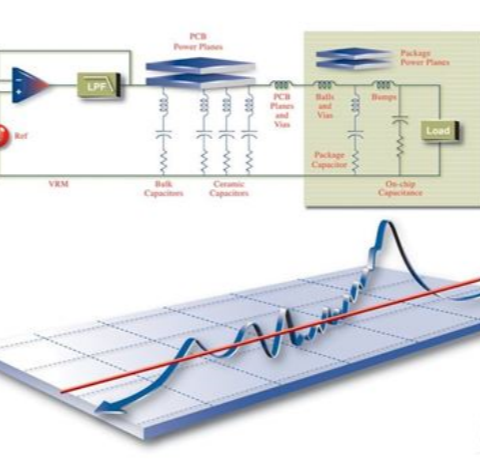
PDN Design Guidelines for HDI PCB: Key Optimization Techniques for Stable Power Delivery
PDN (Power Distribution Network) is a critical part of PCB design, directly determining power delivery efficiency, noise suppression capability, and overall system stability. Skipping PDN simulation a...
Mila
Apr 09,2026
1704
PMU PCB Design Guidelines: Layout and Routing Best Practices for Power Management
The PMU (Power Management Unit) is the core of power supply systems in electronic devices such as smartphones and computers. It is responsible for voltage and current regulation, power switching, batt...
 William Harter
Apr 08,2026
2151
William Harter
Apr 08,2026
2151
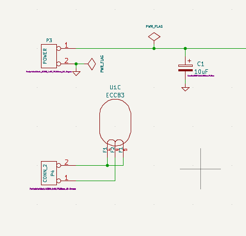
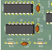
Using Silk Screen
I prefer to include component values, such as 100K and 1 µF, as well as designators like R1 and C1, on the silkscreen of my printed circuit boards. Displaying these values facilitates easier hand asse...
| Ranking | Name | Answers |
|---|---|---|
| 1 | PCBWay Team | 6 |
| 2 | olDirdey | 2 |
| 3 | CezaryCezary | 1 |
| 4 | We're all Geeks | 1 |
| 5 | mike danick | 1 |