 Mila
Apr 17,2026
3904
Mila
Apr 17,2026
3904
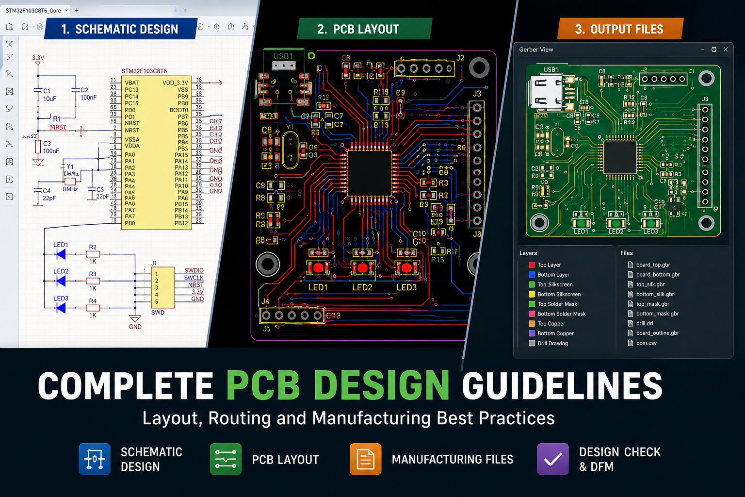
Complete PCB Design Guidelines: Layout, Routing and Manufacturing Best Practices
PCB (Printed Circuit Board) design is critical to the stable operation of electronic products. A well-designed PCB not only ensures signal integrity and reduces electromagnetic interference (EMI), but...
Mila
Jul 27,2026
31
Rigid-Flex PCB Layout Design Guidelines: Best Practices for Reliable PCB Layout
Designing a rigid-flex PCB layout requires a fundamentally different approach than standard rigid boards. The combination of rigid FR4 sections and flexible polyimide (PI) regions introduces unique me...
Mila
Jul 27,2026
62
USB Interface Hardware Design Guide: From Pin Functions to PCB Layout Best Practices
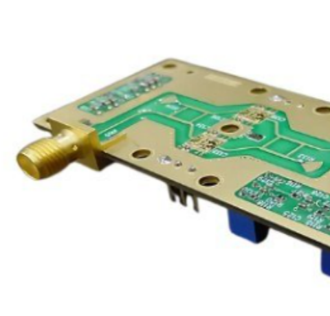
1. Introduction: Never Underestimate USB — A Small Design Mistake Can Cause Major Signal ProblemsIn the eyes of many hardware engineers, the USB interface may seem like a relatively simple peripheral ...
 William Harter
Jul 18,2026
127
William Harter
Jul 18,2026
127
Problem in KiCad footprints that behave as locked when they are not.
Problem In KiCad, some footprints behave as locked even when they are not. For example, when moving a grouped set of footprints on a PCB, most of the footprints move as expected, but one or two may re...
Mila
Jul 03,2026
639
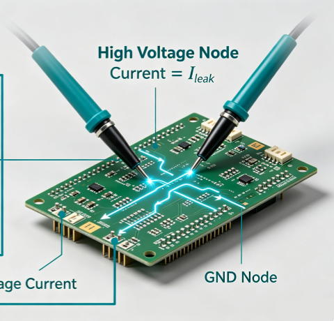
What Causes PCB Leakage Current and How to Reduce Electrical Leakage in Circuits
In high-voltage electronics, medical devices, industrial control systems, and precision measurement circuits, PCB leakage current can significantly affect system stability and measurement accuracy, ev...
Mila
Jun 26,2026
925
Medical PCB Design Guide: Manufacturing, Assembly, Testing, and Industry Standards
As medical electronics continue to evolve toward smarter, smaller, and more connected devices, medical PCB design has become increasingly critical to ensuring product reliability, signal integrity, an...
Mila
Jun 24,2026
526
Understanding ESD Protection in Electronic Systems and PCB Design Practices
Many hardware failures that appear random—such as USB communication errors, MCU resets, touch-screen malfunction, or unexplained field failures—can often be traced back to Electrostatic Discharge (ESD...
Mila
Jun 18,2026
1461
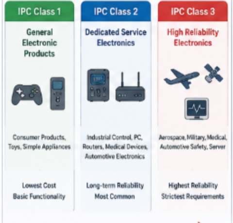
Designing Production-Ready PCBs with IPC Standards
IPC standards are the foundation of modern PCB design, manufacturing, and assembly. By providing a unified set of technical requirements, they help engineers improve reliability, manufacturability, an...
Mila
Jun 17,2026
1161
PCB Annular Ring Design: Sizing, IPC Standards, DFM Rules, and Failure Prevention
In PCB design, the annular ring may seem like a small feature, but it directly affects electrical reliability, solder joint strength, and manufacturing yield. Insufficient annular ring width can lead ...
Mila
Jun 12,2026
1854
RF PCB Design Guide: Layout, Stackup, Routing and Manufacturing Best Practices
RF PCB design is significantly more challenging than conventional PCB design due to the effects of high-frequency signal propagation, impedance discontinuities, and electromagnetic interference. Even ...
Mila
Jun 09,2026
749
Circuit Symbols Explained: A Complete Guide to Electronic Symbols and Schematic Symbols in PCB Design
In electronic product development, hardware design, equipment maintenance, and PCB design, schematic diagrams serve as the essential bridge between design, manufacturing, and debugging. At the core of...
Mila
Jun 04,2026
1176
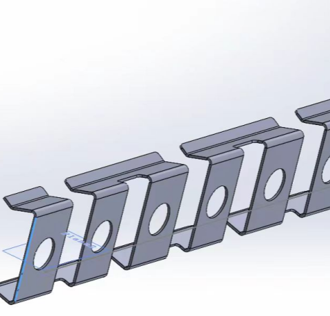
Sheet Metal Bending Design Guide: DFM Rules, Bend Radius, Bend Allowance, and Manufacturing Best Practices
Although sheet metal bending appears to be a simple manufacturing process, many production issues—including cracking, hole distortion, tooling interference, excessive springback, and assembly failures...
Mila
May 28,2026
1048
Sheet Metal Box Design Guide: 12 Common DFM Mistakes to Avoid
Sheet metal fabrication is widely used for enclosures, brackets, chassis, and industrial housings through processes such as cutting, bending, welding, and surface finishing. Although many designs look...
Mila
May 26,2026
2085
Complete Sheet Metal Box Design Guide for Electronic Enclosures
With the advantages of controllable cost, reliable strength, and efficient manufacturing, sheet metal enclosures are widely used in electronics, industrial control, telecommunications, medical equipme...
 Engineer
May 22,2026
1449
Engineer
May 22,2026
1449
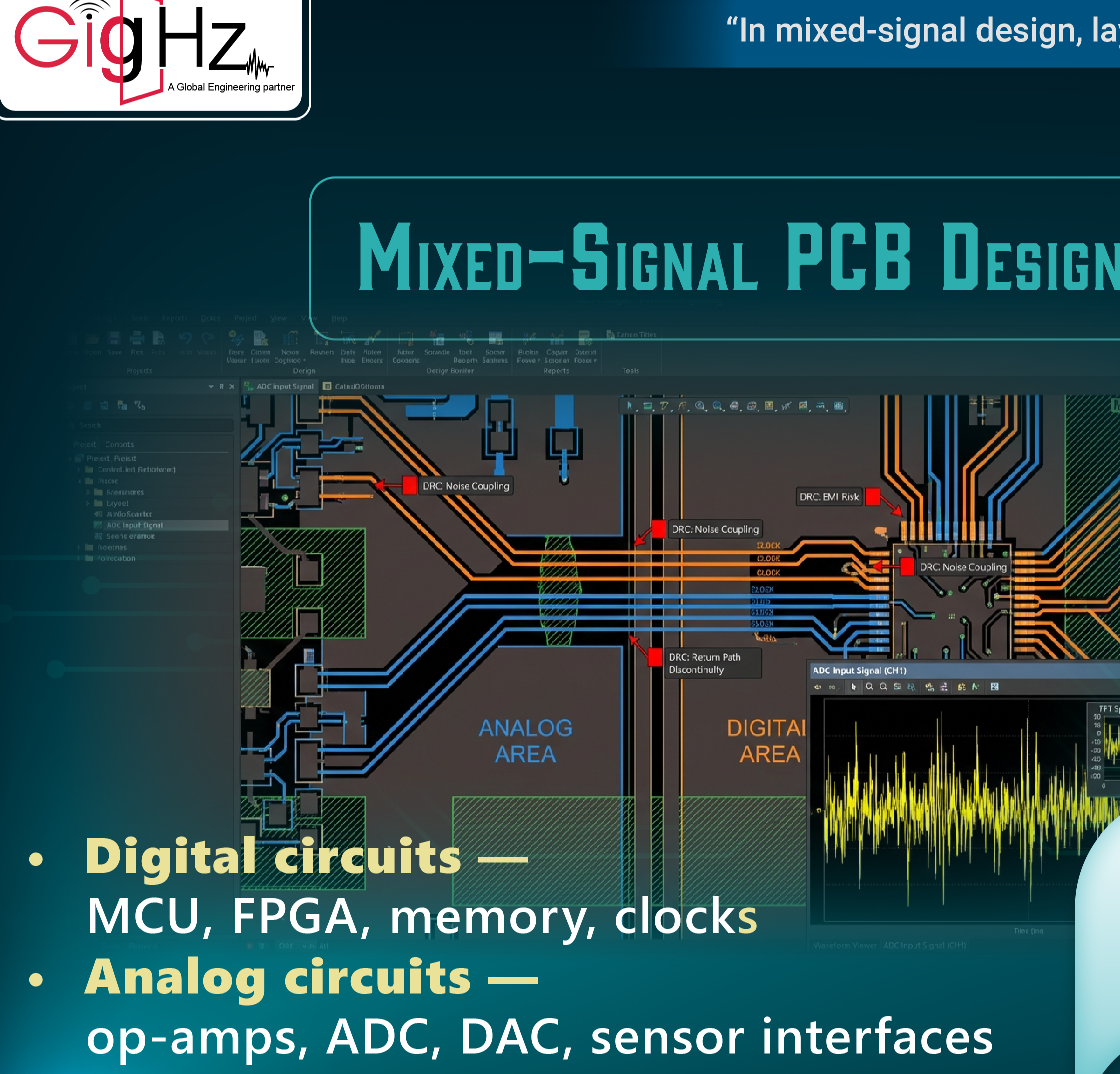
Mixed-Signal PCB Design: A Practical Engineering Guide
Mixed-Signal PCB Design: A Practical Engineering GuideMany PCB performance issues are not caused by firmware or components — they originate in the layout itself.When a mixed-signal board shows unstabl...
Mila
May 21,2026
3111
Decoupling Capacitor Placement Guidelines for High-Speed PCB Design
Many high-speed PCBs appear correct during schematic design, yet after fabrication, problems such as FPGA configuration failures, unstable DDR timing, ADC noise, EMC radiation issues, and excessive po...
Mila
May 18,2026
2782
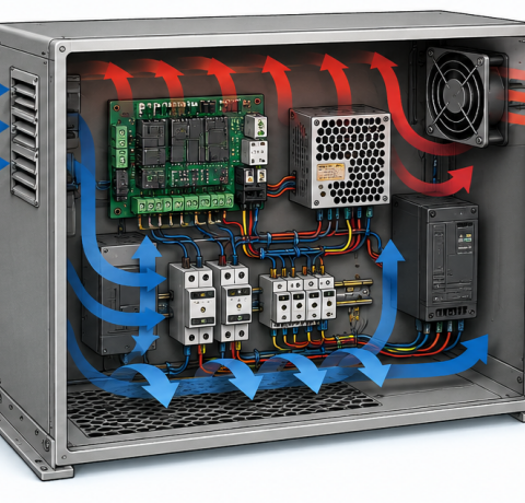
Electronic Enclosure Thermal Management: Cooling Design and Best Practices
Enclosure thermal management is critical for preventing overheating, condensation, and premature electronic component failure. A well-designed enclosure cooling system helps maintain stable operating ...
Mila
May 14,2026
3455
EMI Shielded Enclosure Design Guide: Principles, Materials, and Best Practices
EMI (Electromagnetic Interference) has become a major challenge in modern electronic systems. In many projects, EMI-related issues do not appear during early development, but instead emerge during EMC...
Mila
May 11,2026
3387
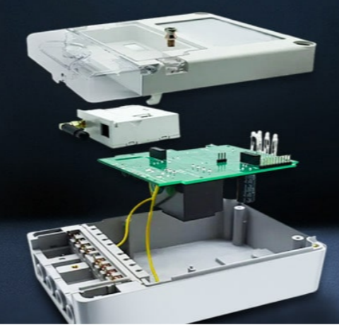
PCB Enclosure Design Guide: Materials, IP Ratings, and Structural Best Practices
In electronic product development, enclosure design is often underestimated. Even when the PCB functions correctly, poor enclosure design can still lead to overheating, assembly interference, insuffic...
Mila
May 07,2026
1821
Basic PCB Design: Complete PCB Design Guidelines for Beginners
PCB is the core carrier of modern electronic devices. From wearable products to servers and automotive electronics, reliable PCB design is essential to system performance and stability. Many beginners...
| Ranking | Name | Answers |
|---|---|---|
| 1 | PCBWay Team | 7 |


