High Current PCB is a special type of circuit board designed to carry large amounts of current. Compared to ordinary PCBs, it can handle more power, which makes it indispensable in many high-power applications.
In today’s world, the devices we use are more powerful than ever — think of electric vehicles, industrial machinery, and high-power LED lighting. These devices require strong and stable power to function properly. Without a high current PCB, these high-power systems could overheat, fail, or even become hazardous.
A high current PCB layout ensures power is delivered safely and efficiently. The importance of high current trace design lies in the fact that it directly determines the safety, reliability, and performance of the product. Unlike signal traces, high current traces are not simply “connected and done.” They must be treated as structural elements with resistance, inductance, and thermal characteristics.
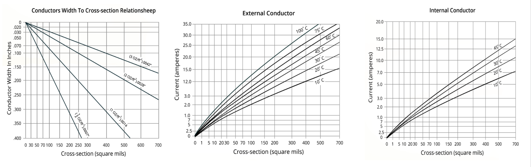
Start from the required current. Some online calculators can help with this. Enter the current value, and they’ll tell you the correct PCB Trace Width. For high current PCB layout, wider traces are better — they reduce resistance and keep the board temperature lower.
Use the IPC-2152 standard chart or an online current-carrying capacity calculator to determine the minimum width under different temperature rise conditions.
Thicker copper layers can carry more current. Formula:
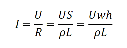
(I = allowable current, U = voltage, R = resistance, S = cross-sectional area, ρ = resistivity, L = trace length, w = trace width, h = trace thickness.)
Under the same conditions (especially fixed trace width), the allowable current I is proportional to the copper thickness h — the thicker the copper, the higher the current capacity.
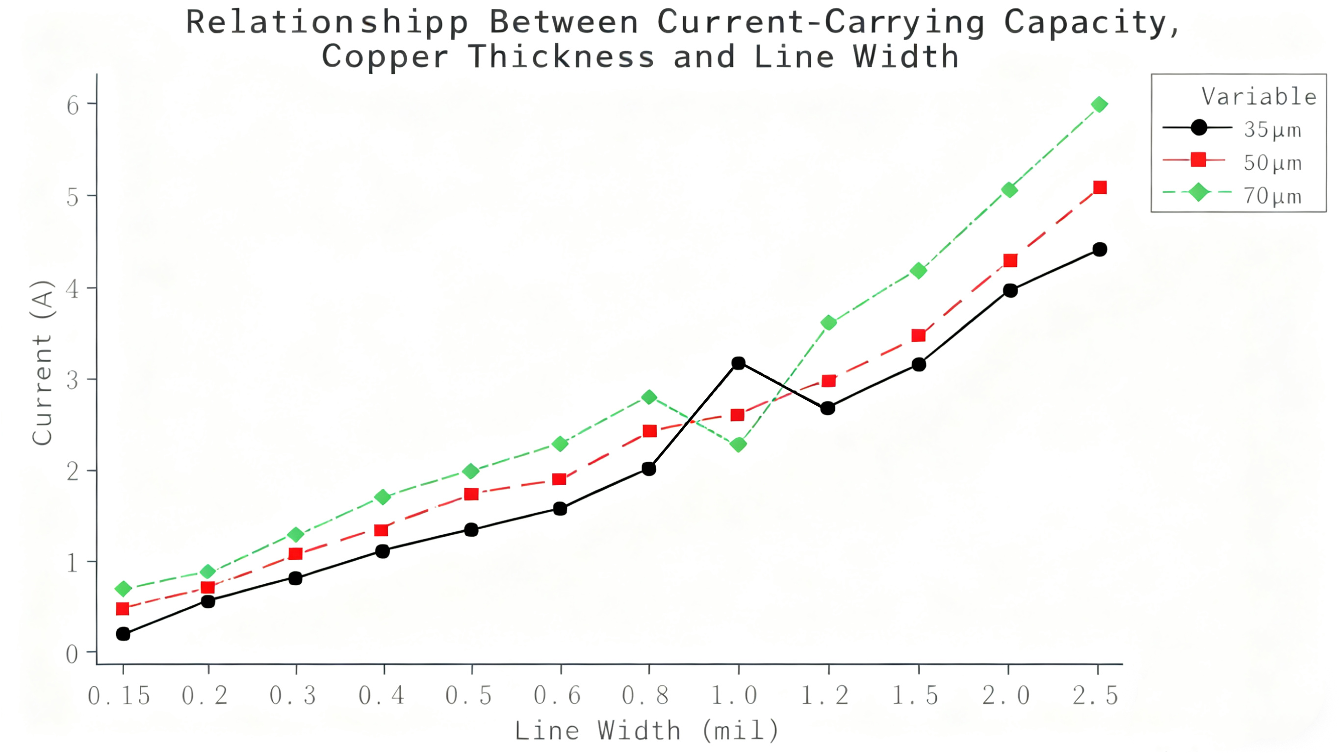
(Correlation between current carrying capacity, copper thickness and line width)
If the current is very large, apply power copper pours on the top, bottom, and inner layers, then connect them with via arrays in parallel. This is one of the most powerful high current routing techniques in multilayer power PCB design.
Distribute high current traces across multiple layers to spread the heat. This helps maintain a cooler and more efficient high current PCB layout.
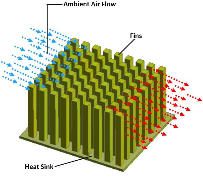
A heatsink is a metal component attached to the PCB that helps dissipate heat. In high current PCB design, heatsinks are often necessary to prevent overheating and to ensure the board operates within safe temperature limits.
Copper fill (large copper areas) helps improve heat dissipation. By spreading heat evenly, copper pours keep the power PCB design thermally stable. In high current applications, this is crucial to prevent overheating and voltage drop in PCB traces.
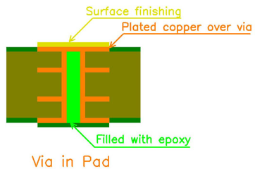
Via Design for High Current
Never use a single via to connect high current layers. Estimate via current capacity (approximately 1A per 0.4 mm hole) and use via arrays to distribute the load.
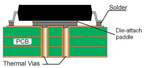
Larger via diameters (e.g., 0.3–0.5 mm) have thicker copper plating and therefore higher current-carrying capacity. This is a key part of high current via design.
If possible, request the manufacturer to fill vias with conductive epoxy or plate them with solder, which improves both current capacity and heat conduction.
Keep traces as short as possible. Longer traces have higher inductance, which increases voltage spikes. Short traces maintain stable current flow and reduce losses — a crucial tip in high current trace design.
Use 45° bends or rounded corners instead of 90° turns. Sharp angles increase inductance and can accumulate charge at high frequencies.

A ground plane is a large copper area connected to ground. It helps reduce inductance and improves PCB stability. Using power and ground planes together creates a low-impedance path for current flow, minimizing EMI and enhancing performance in high current PCB layout.
Keep power and ground traces close to each other to minimize loop area, reduce inductance, and lower electromagnetic interference (EMI).
Place components that handle high current close to each other to shorten the current path. Shorter paths generate less heat and reduce energy loss, improving overall efficiency and reliability in power PCB design.
A high current PCB is vital for high-power applications. It ensures devices operate efficiently and reliably, extending the durability and stability of electronic systems. Whether used in industrial equipment, automotive systems, solar power stations, or offshore wind farms, a high current PCB layout is the backbone of system performance and high current trace reliability.


