1. Blog>
  2. DDR2 PCB Layout Guidelines: Routing, Termination, and Design Principles

DDR2 PCB Layout Guidelines: Routing, Termination, and Design Principles

by: Feb 25,2026 31 Views 0 Comments Posted in PCB Design & Layout

ddr2 pcb layout ddr2 pcb layout design ddr2 pcb design ddr2 pcb layout guidelines

In modern high-speed digital circuit design, DDR2 memory remains a widely used high-speed storage device. Due to its high operating frequency, the quality of the DDR2 PCB layout directly determines whether the hardware system can function reliably and how fast it can operate. Poor routing may lead to signal integrity degradation, timing violations, or even complete system failure.

This article discusses the key considerations for DDR2 PCB routing, including impedance control, termination design, routing sequence, and topology comparison with DDR3.


DDR Routing Termination Design Considerations

Impedance Control

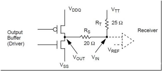
The single-ended impedance should be controlled at 50Ω (±10%), while the differential impedance should be 100Ω (±10%), ensuring proper signal integrity and minimizing reflections.


Reference Plane Selection

  • DQ, DQS, and clock signals are recommended to use VSS (GND) as the reference plane to achieve a stable return path and reduce jitter.
  • Address, command, and control signals may use either VDD or VSS as the reference plane, but priority should be given to maintaining plane continuity and avoiding routing across split planes.


Termination Techniques

  • Series Termination

Series termination is mainly suitable for cases with lighter loads or strong driver capability. For unidirectional signals such as address and control lines, the series resistor should be placed close to the signal driver, which helps suppress reflections and improve signal quality.

  • Parallel Termination

When the load is heavy, the routing is long, or simulation indicates the need for additional matching, parallel termination can be used. The termination resistor is typically connected to the termination voltage VTT, with a common resistance range of 36Ω–56Ω, and 47Ω is often selected as a typical engineering value.

  • Differential Termination

Differential clock signals (CK/CK#) require 100Ω differential termination, which can be implemented using internal ODT (On-Die Termination) or external resistors.


DDR2 Routing Sequence and Length Matching Principles

Routing Priority

In a proper DDR2 PCB layout, the recommended routing order is:

  1. Power and reference plane planning (VDD, VDDQ, VTT)
  2. Clock signals (CK/CK#)
  3. Data strobe signals (DQS)
  4. Data signals (DQ, DM)
  5. Address, command, and control signals
  6. Power network optimization and reinforcement

Prioritizing critical high-speed signals helps ensure timing margin and signal integrity across the entire system.


Clock Routing Rules

  • Differential pair intra-pair matching: ≤ 50 mil (tighter is recommended)
  • Differential spacing: ≥ 3× trace width
  • Length difference between clock pairs: ≤ 100 mil
  • Maintain a continuous reference plane and avoid crossing plane splits


Data Group Routing Rules

Each Data Group (DQ[7:0] + DQS + DM) should satisfy:

  • Signals within the same byte lane should preferably be routed on the same layer
  • DQ length matching relative to DQS: ≤ 50 mil
  • Length difference between byte lanes: ≤ 1000 mil
  • Matching between DQS and CK is less strict, typically within 500–1000 mil

Since DDR2 data and DQS operate in a source-synchronous manner, DQS serves as the length-matching reference within each group.


Address, Command, and Control Signals

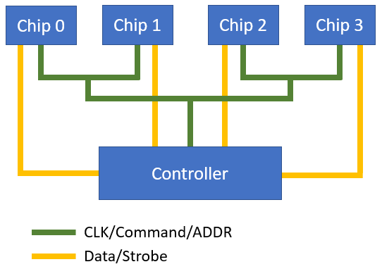
In a DDR2 T-branch topology:

  • Address, command, and control signals operate as source-synchronous interfaces
  • Group length matching is required, but with lower accuracy than data groups
  • Typical matching within ±100 mil is sufficient
  • Signal lengths may be slightly longer than the clock but should avoid excessive deviation


Termination and VTT Power

When the DDR2 load is heavy or multiple memory devices are used, the design should include:

  • Parallel termination resistors
  • A VTT termination power network

These measures reduce reflections and improve signal integrity.


DDR2 vs DDR3 Layout Differences

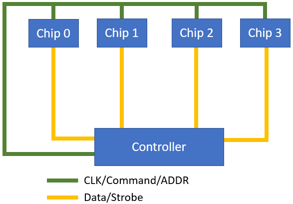
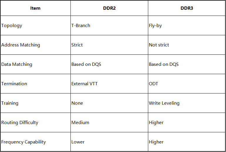
In a previous article, we introduced DDR3 Routing Guide. The differences between DDR2 and DDR3 layouts are primarily caused by topology changes (T-branch → Fly-by). Before reviewing the comparison table, the following topology diagrams help illustrate the concept.


DDR2 Topology (T-Branch)

Characteristics:

  • Address and command signals branch to each memory device
  • Strict length matching is required
  • Larger stubs
  • Limited frequency capability


DDR3 Topology (Fly-by)

Characteristics:

  • Address and command signals are routed sequentially through each device
  • Unequal trace lengths
  • Requires training mechanisms (Write Leveling)
  • Supports higher operating frequencies


DDR2 vs DDR3 Routing Comparison


If you need assistance with PCB design or PCB layout, feel free to contact the PCBWay Design Team!

Join us
Wanna be a dedicated PCBWay writer? We definately look forward to having you with us.
  • Comments(0)
Upload photo
You can only upload 5 files in total. Each file cannot exceed 2MB. Supports JPG, JPEG, GIF, PNG, BMP
0 / 10000
    Back to top