The quality of a DC-DC converter design is determined not only by the chosen topology and component parameters, but very often by the PCB layout, which can ultimately decide the success or failure of the design. Even when the schematic is correct, a poorly executed PCB layout may lead to increased circuit sensitivity, degraded EMC performance, and in severe cases, malfunction or even component damage.
Therefore, an excellent DC-DC power design can be characterized by a few core criteria: high operational stability, strong immunity to interference, and compliance with EMC requirements while meeting electrical specifications. These performance factors are highly interdependent—any improper handling of a single detail may trigger a chain reaction that compromises the entire system. In practical engineering, PCB layout is frequently the primary source of such issues.
This article highlights several key layout considerations for achieving a robust DC-DC converter PCB layout.
The smaller the power loop area, the lower the parasitic inductance, making switching noise and EMI easier to control. Power loops should be kept short, straight, and clearly closed, avoiding unnecessary detours and loop expansion to reduce radiated noise.
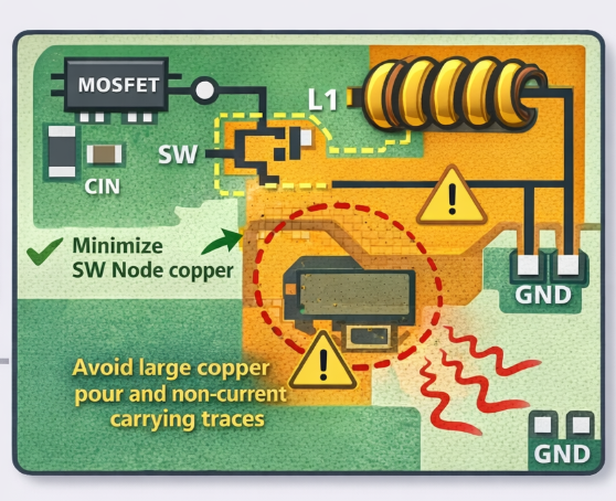
The switching node (SW) is a major noise source; while ensuring sufficient current capability, its copper area should be kept as small as possible and placed away from sensitive and interference-prone signals. For example, the inductor should be placed close to the SW pin and away from feedback traces. The output capacitor should be located close to the inductor, with additional ground vias provided at the ground terminal to improve current return paths.
Within the power loop, special attention must be paid to the thermal (hot) loop. The thermal loop is formed during the switching process due to rapid changes in current, and it has a significant impact on EMI noise generation in DC/DC converters. By minimizing the thermal loop area, keeping routing short and direct, and isolating it from sensitive signal regions, EMI can be significantly reduced and system stability improved.
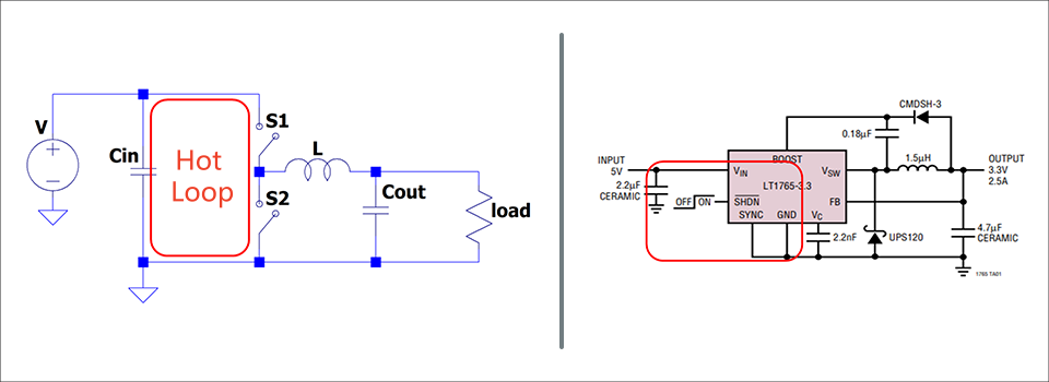
(Thermal Loop of a Step-Down DC/DC Converter)
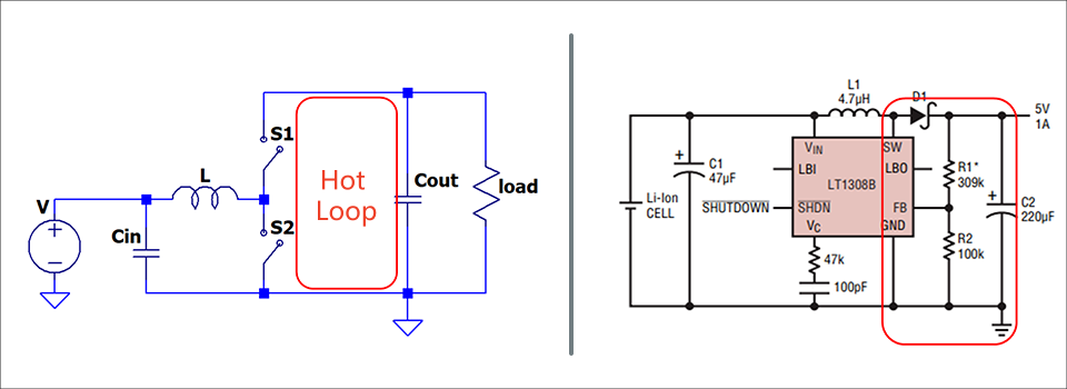
(Thermal Loop of a Step-Up DC/DC Converter)
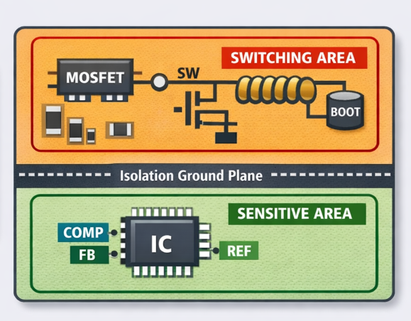
In DC-DC converters, compensation networks and voltage feedback sensing circuits are highly sensitive nodes that are easily affected by switching noise and are among the most common causes of system instability. Therefore, these circuits should be physically separated from noise sources such as the SW node, inductors, and diodes (in non-synchronous buck converters). Proper functional zoning helps reduce electromagnetic coupling and interference.
In recommended layouts, the compensation and feedback circuits are placed in relatively “quiet” areas, well away from switching nodes, which effectively enhances system stability and noise immunity.
The layout and routing of the inductor are critical factors in determining the EMI performance of a DC-DC power supply, particularly with respect to radiated emissions, yet their importance is often underestimated. The inductor itself is a primary source of high-frequency magnetic field noise, while the associated switching node (SW node) is a high dv/dt voltage transition node. If the layout and routing are not properly handled, this area can easily act as an efficient “antenna,” leading to severe radiated interference as well as increased conducted noise.
These issues are often difficult to identify at the schematic design stage, but they may become a primary cause of EMC test failures during PCB implementation.
The PCB layout of a DC-DC converter is a critical factor in determining power supply performance and reliability. An effective layout focuses on controlling noise and current paths: high-frequency, high-current loops should be made as compact as possible to suppress EMI, while sensitive feedback and control signals must be strictly isolated to prevent interference. At the same time, clear separation and planning of power ground and signal ground, along with proper placement of key components and thermal considerations, together form the physical foundation of a stable, efficient, and low-noise power supply.
The core of DC-DC PCB layout is “noise and current loop control,” while the core of AC-DC PCB layout is “safety and isolation.” If you’ve finished reviewing the key DC-DC PCB design considerations and would like to learn more about AC-DC PCB layout, you can continue with the following article: AC-DC PCB Layout Guidelines: Safety, Isolation, and EMI Control
If you need the help of the DC-DC converter PCB layout, you can contact PCBWay design team to help you!


