EMI (Electromagnetic Interference) has become a major challenge in modern electronic systems. In many projects, EMI-related issues do not appear during early development, but instead emerge during EMC testing, product certification, or field deployment, often resulting in redesigns, structural modifications, delayed product launches, and additional compliance costs.
With experience across PCB layout, enclosure engineering, and manufacturability optimization, PCBWay enclosure design service has supported a wide range of projects involving EMI shielded enclosure design, EMC optimization, and high-speed electronic systems.
EMI (Electromagnetic Interference) involves two core issues: unwanted emissions from electronic devices and susceptibility to external interference. These problems can cause data errors, communication instability, intermittent failures, and EMC compliance issues.
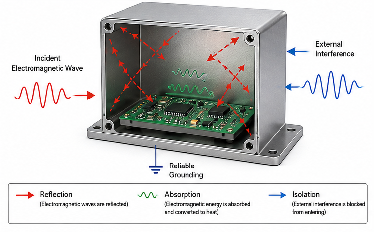
An EMI shielded enclosure is based on the Faraday Cage principle. It uses conductive or magnetic materials to form a continuous shielding structure, containing internal radiation while blocking external interference.
For this reason, EMI enclosure design is widely used in high-speed electronics, industrial systems, medical devices, and communication equipment.
Shielding performance is measured using Shielding Effectiveness (SE), expressed in dB. Typical requirements vary by application:
EMI shielding is achieved through three main mechanisms: reflection (reducing electric-field interference), absorption (converting energy into heat), and multiple reflection (further attenuation inside the material).
EMI risks are often underestimated during early product development. However, the following scenarios typically require EMI shielding design from the beginning of the project:
Many EMI shielding failures are caused by structural leakage rather than shielding material limitations. Seams, openings, and fastening areas are among the most common EMI leakage paths.
As a result, structural details are often more important than simply using higher-grade shielding materials.
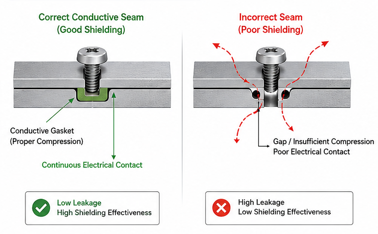
(1) Seam Design and Electrical Continuity
Enclosure seams are one of the largest sources of high-frequency EMI leakage. Even microscopic gaps can significantly reduce shielding effectiveness.
Key design considerations include:
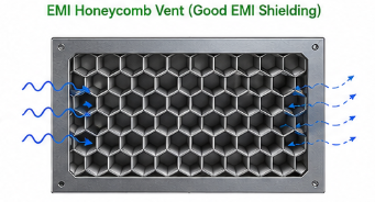
(2) Ventilation and Opening Design
Electronic devices often require ventilation holes, cable exits, or display openings. However, these features can also become major EMI leakage paths.
Opening dimensions should generally follow the waveguide cutoff principle, meaning the opening size should remain below approximately 1/20 of the interference wavelength.
Practical design recommendations include:
(3) Internal Partitioning and Grounding Design
Proper internal partitioning and grounding can significantly reduce electromagnetic coupling between different circuits.
Common practices include:
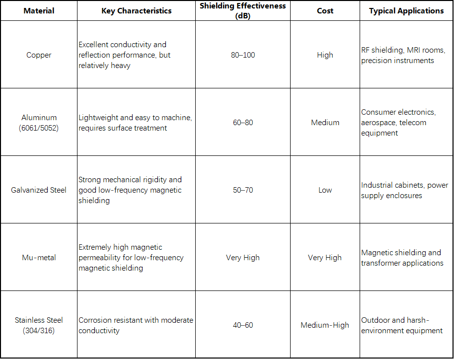
Shielding materials directly affect the upper limit of EMI shielding effectiveness. Material selection should consider interference frequency, shielding requirements, environmental conditions, weight, manufacturing processes, and overall cost.
(1) Metal Materials for EMI Shielded Enclosures
(2) Plastic EMI Shielding Solutions
Plastic enclosures do not inherently provide EMI shielding and therefore require additional conductive treatment.
Common solutions include:
These approaches are suitable for lightweight and complex enclosure designs, although their shielding performance is typically lower than fully metallic EMI shielded enclosures.
(3) Material Selection Challenges
EMC compliance is mandatory for most electronic products entering commercial markets. Different industries and regions require different EMI shielding standards.
Common standards include:
Many EMI shielding failures are caused by overlooked engineering details rather than theoretical errors.
Common mistakes include:
Successful EMI enclosure design should be integrated into the entire product development process rather than treated as a late-stage correction.
A typical workflow includes:
As electronic systems continue moving toward higher speeds, smaller form factors, and greater power density, EMI shielded enclosure design is becoming an essential engineering capability rather than an optional optimization step.
For projects requiring enclosure engineering, EMC optimization, PCB layout, or manufacturability support, PCBWay enclosure design service can help streamline development, reduce redesign risks, and improve overall product reliability from prototype to production.


