PCB (Printed Circuit Board) design is critical to the stable operation of electronic products. A well-designed PCB not only ensures signal integrity and reduces electromagnetic interference (EMI), but also improves thermal performance and manufacturability.
Based on practical engineering experience, this article provides a complete set of actionable PCB design guidelines, covering the full design process to help engineers build high-performance and reliable PCB solutions.
Before starting PCB layout, it is essential to define design rules. This step bridges design and manufacturing, and helps prevent costly redesigns. In practice, PCB design is fundamentally about controlling signal paths, current return loops, and energy distribution. Design rules serve to constrain these factors from the very beginning.
Define minimum trace width, spacing, via size, and pad dimensions based on PCB manufacturer capabilities. Via hole size and pad dimensions must match fabrication limits to avoid defects such as open vias or poor solder joints. You can check PCBWay’s manufacturing capabilities to make your PCB design process easier.
For 1 oz copper with a 10°C temperature rise, a 1A current typically requires a trace width of approximately 0.3–0.5 mm (based on IPC-2152).
Select the stackup based on signal speed, component density, and cost:
Key principles:
A proper stackup also ensures a stable return path for signals.
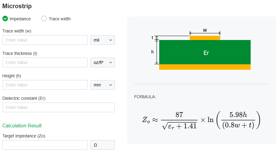
Define impedance requirements in advance:
Also, calculate trace widths for high-current paths based on IPC-2152 to prevent overheating and voltage drop. Here is PCBWay's free Impedance Calculation tool you can use.
Component placement directly impacts signal integrity, thermal performance, and manufacturability. The key principles are functional partitioning, signal prioritization, and thermal optimization.
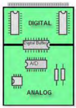
Separate analog, digital, and power circuits to minimize interference.
Physically isolate high-frequency and low-frequency components. Place clock and RF modules away from I/O connectors to reduce external coupling.
Why it matters:
High di/dt noise from digital circuits can couple into analog circuits through shared return paths.
Place processors, FPGAs, and high-speed interface chips close to connectors and signal sources to minimize trace length.
Decoupling capacitors should be placed as close as possible to power pins (typically < 2–3 mm) to ensure low-inductance current loops and stable power delivery.
For more detailed decoupling capacitor placement guidelines, including stackup optimization, SRF matching, BGA decoupling strategies, and PDN considerations, you can also read:
Decoupling Capacitor Placement Guidelines for High-Speed PCB Design
Keep heat-generating components away from temperature-sensitive devices such as electrolytic capacitors and crystals.
Place large components centrally, with smaller components arranged around them. Keep SMD components on the same side whenever possible to simplify assembly.
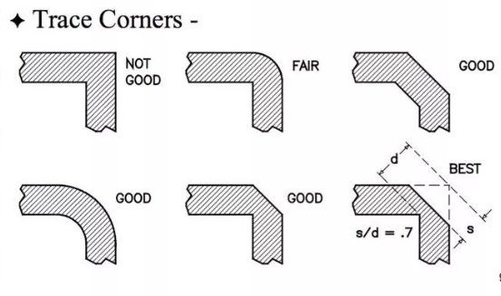
Routing is the core of PCB design, focusing on signal integrity, impedance control, crosstalk reduction, and power delivery.
In high-speed designs (>5 Gbps): Via stubs can create resonant structures, increasing insertion loss and degrading signal integrity. Backdrilling is often required to eliminate via stubs.
It is recommended that keep PCB surface temperature rise within 20°C, and maintain at least 20–30°C margin below maximum junction temperature.
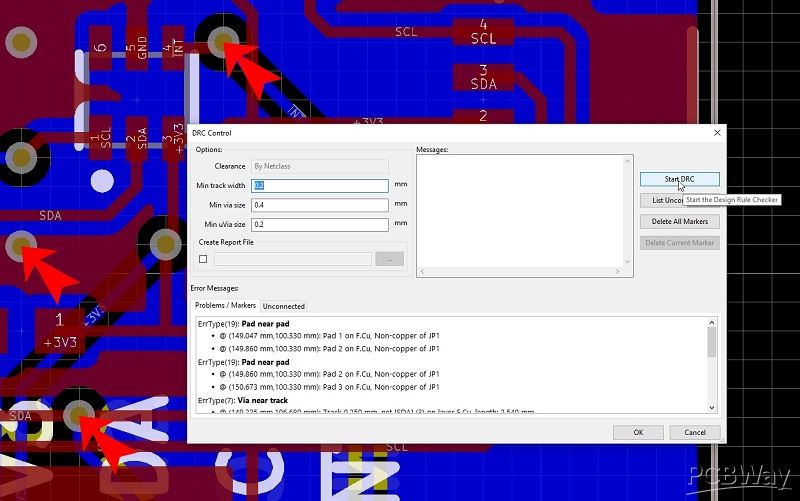
After completing the design, it is essential to verify manufacturability, assembly feasibility, and electrical correctness. A well-designed PCB is not only electrically correct, but also manufacturable, assembly-friendly, and fully validated before production.
You can use PCBWay free DRC tool to check:
PCB design is fundamentally about controlling signal paths, current loops, and energy distribution. Proper layout, disciplined routing, and optimized stackup together determine the overall performance of a PCB.
In real-world projects, PCB design is not only about schematic capture and routing, but also involves signal integrity, power distribution, EMC, thermal management, manufacturability, and production reliability.
For engineers or teams working on complex, high-speed, RF, HDI, or production-oriented projects, PCBWay PCB Design and Layout Service provides professional support covering schematic design, PCB layout, firmware development, enclosure design, and manufacturing preparation — helping reduce redesign risks and improve first-pass success rate. You can get a free quote through PCBWay’s online PCB design service platform.


