1. Blog>
  2. Mixed Signal PCB Design: Common Interference Issues and Practical Solutions

Mixed Signal PCB Design: Common Interference Issues and Practical Solutions

by: Apr 07,2026 350 Views 0 Comments Posted in PCB Design & Layout

mixed signal pcb design mixed signal pcb layout mixed signal pcb design guidelines mixed signal circuit design

In electronic design, interference in mixed-signal systems is a common challenge for engineers. Digital circuits have strong noise immunity, while analog circuits are highly sensitive—even minor interference can significantly degrade system performance or cause failure. Based on extensive engineering experience, the PCBWay design team summarizes key considerations for mixed signal PCB design in this article.


Core Differences Between Analog and Digital Signals

The root cause of interference in mixed signal PCB design lies in the fundamental differences between analog and digital signals. When they coexist, digital noise can easily “contaminate” the analog domain and even lead to EMI issues.

  • Analog signals are continuous and represent physical quantities such as temperature, pressure, sound, and images. They require high signal integrity.
  • Digital signals are discrete and quantized, such as text, graphics, and video in computing systems. Their high-speed switching characteristics tend to generate noise. 


Common Sources of Interference in Mixed Signal PCB Design

In practical mixed signal PCB design, interference mainly comes from four aspects, all closely related to signal routing, power distribution, grounding, and layout strategy:

  • Inductive coupling from digital signal lines to analog circuits

Poor partitioning and routing can cause digital signal currents to induce electromagnetic interference, disrupting the continuity of analog signals.

  • Coupling from digital power and ground to analog circuits

Although analog and digital grounds share a common reference, improper design allows digital noise to couple into analog circuits through parasitic capacitance, degrading accuracy.

  • Interference between analog subcircuits

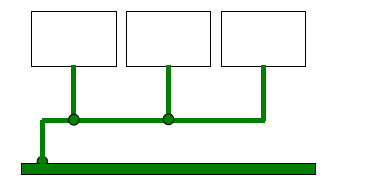
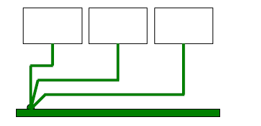
When multiple analog modules share the same ground or power path, common impedance coupling may cause crosstalk and reduce system efficiency.

  • Signal masking in analog transmit/receive circuits

Strong transmit signals can overwhelm weak receive signals if proper isolation is not implemented, leading to signal loss at the receiver. 


Optimization Techniques for Mixed Signal PCB Design

To mitigate these interference issues, optimization in mixed signal PCB design should focus on four key areas: layout, grounding, power management, and circuit isolation. The goal is to keep the analog domain “quiet” while ensuring efficient digital operation.

1. Partitioned Layout to Minimize Coupling

A clear physical separation between analog and digital sections is essential in mixed signal PCB design.

  • Define distinct analog and digital areas on the PCB.
  • Place ADC/DAC devices at the boundary, preferably closer to the analog side.
  • Avoid crossing analog and digital signal traces.
  • Prevent high-speed digital traces from routing above or below sensitive analog components.
  • Follow natural signal flow and avoid unnecessary routing complexity.


2. Proper Grounding to Avoid Common Impedance Coupling

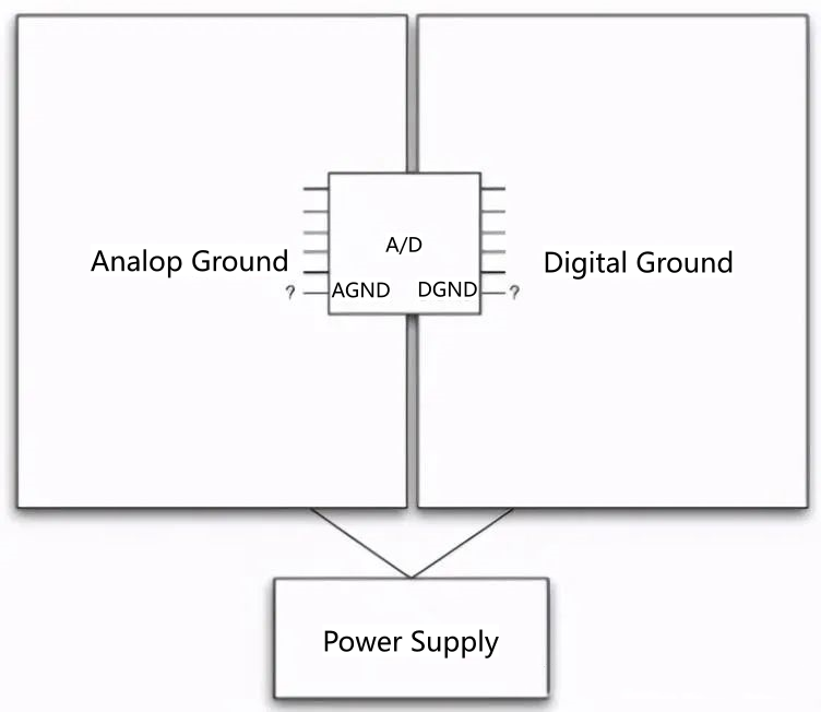
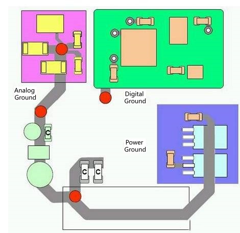
Grounding is one of the most critical aspects of mixed signal PCB design. The objective is to maintain a unified reference while preventing digital noise from entering the analog ground.

  • Series single-point grounding: Simple, suitable for low-complexity systems, but may introduce common impedance coupling.

  • Parallel single-point grounding: Eliminates common impedance coupling but increases routing complexity.

  • Practical approach: Use partitioned copper pours for analog and digital grounds, then connect them at a single point (e.g., under ADC/DAC ground pins or near the power entry) using a 0Ω resistor or ferrite bead.


3. Power Isolation to Block Noise Propagation

Power integrity is crucial in mixed signal PCB design, as noise can easily propagate through power planes.

  • Separate power supplies: Ideally, use independent power rails for analog and digital sections, even if they share the same voltage level.
  • Filtering components: Use ferrite beads, LC filters, or low-noise LDOs at power entry points for each domain.
  • Decoupling capacitors: Place them close to IC power pins to suppress both high- and low-frequency noise.


4. Circuit Isolation to Reduce Coupling Paths

Targeted isolation techniques help minimize interference between different circuit blocks:

  • Analog subcircuit isolation: Use single-point grounding or ferrite beads to isolate power and ground paths between modules.
  • Transmit/receive isolation: Maintain sufficient physical distance, use ground shielding, and isolate power supplies to prevent strong signals from overwhelming weak ones. 


Conclusion

Effective mixed signal PCB design requires a systematic approach centered on partitioning, grounding, and isolation. It is not a single design adjustment but a coordinated effort across layout, grounding strategy, power distribution, and circuit isolation.

By carefully managing signal paths and minimizing noise coupling at every stage, engineers can significantly improve both the stability and accuracy of mixed signal systems, ensuring reliable and high-performance designs.


For reliable mixed signal PCB design, the PCBWay design team can help you optimize layout, grounding, and noise performance based on real-world experience. Contact us to turn your design into a production-ready solution.

Join us
Wanna be a dedicated PCBWay writer? We definately look forward to having you with us.
  • Comments(0)
Upload photo
You can only upload 5 files in total. Each file cannot exceed 2MB. Supports JPG, JPEG, GIF, PNG, BMP
0 / 10000
    Back to top