In multilayer PCB design, there is a widely accepted guideline: power planes should be slightly smaller than ground planes, with a uniform edge inset instead of matching the board outline.
Many engineers follow this rule in practice, but not everyone fully understands the underlying physics, when it actually matters, and how to apply it correctly in real projects.
Based on our experience, the PCBWay design team has summarized key insights on power plane layout in this article—from theory to practical implementation.
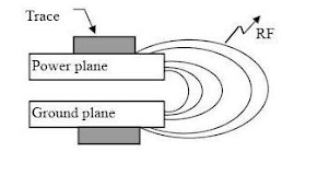
At its core, the issue comes down to one thing: edge-field radiation. A power plane and its adjacent ground plane essentially form a large parallel-plate capacitor. When current switches rapidly, an alternating electric field is established between the two planes.
In conclusion, the stronger the edge field, the harder it is to control EMI.
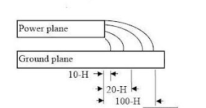
One of the most well-known solutions in the industry is the 20H rule:
By applying this rule:
In essence, the ground plane suppresses edge electric fields and reduces their radiation from the PCB boundaries.
Although the 20H rule is theoretically sound, it is rarely applied strictly in real designs. The reasons are practical:
Therefore, in practice, a more practical compromise is usually adopted:
Although the 20H rule is effective, it only delivers meaningful results under the right conditions. Otherwise, its impact can be minimal.
The layers directly above and below the power plane should both be GND to provide effective field containment.
In 4-layer or lower stackups, the power plane is often located near the outer layers, limiting the effectiveness of the 20H rule. In these cases, EMI control relies more on grounding, shielding, and filtering.
For low-frequency, low-speed, or small-signal designs, the impact of plane inset is usually minimal. In such cases, power integrity should take priority.
Any splits, gaps, or slots in the ground plane can significantly degrade EMI performance—often far more than not shrinking the power plane.
Avoid uneven setbacks (e.g., large inset on one side and minimal on another). A consistent margin provides better results.
Even with proper power plane inset, high-speed signals routed near the PCB edge can still radiate. Critical signals should be placed on inner layers whenever possible.
Achieving good EMI performance requires more than plane inset. Effective grounding of the chassis or metal enclosure, along with shielding, is essential.
Shrinking the power plane slightly relative to the ground plane helps reduce edge-field radiation and improve EMI. In practice, a 0.5–1 mm margin is usually sufficient, provided the ground plane is intact and the stackup is properly designed. Combined with careful routing and grounding, this simple adjustment enhances both performance and manufacturability.
If you need assistance with PCB layout, the PCBWay design team is ready to help.


