Summary: Many PCB performance issues are not caused by firmware or components — they originate in the layout itself. When a mixed-signal board shows unstable ADC readings, EMI failures, unexpected noise, or inconsistent measurements, the root cause is usually physical design decisions made during PCB layout. Mixed-signal design requires more than separating analog and digital sections.
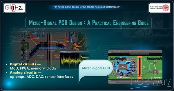
Many PCB performance issues are not caused by firmware or components — they originate in the layout itself.
When a mixed-signal board shows unstable ADC readings, EMI failures, unexpected noise, or inconsistent measurements, the root cause is usually physical design decisions made during PCB layout.
Mixed-signal design requires more than separating analog and digital sections. It requires careful control of grounding, routing, placement, and return current paths so both domains can operate without interference.
This guide explains practical, engineering-focused techniques to improve mixed-signal PCB performance.
A mixed-signal PCB integrates both digital and analog circuitry on the same board.
Digital circuits: MCU, FPGA, memory, clocks, communication interfaces
Analog circuits: ADC, DAC, op-amps, sensor interfaces
Digital circuits switch at high speed and generate noise.
Analog circuits process low-level signals and are highly sensitive to interference.
The challenge in PCB design is ensuring both coexist without degrading each other’s performance.
In real-world designs, common issues include:
· Fluctuating ADC readings
· Increased noise floor in measurements
· Audio or sensor signal distortion
· EMI test failures
· Unstable or inconsistent outputs
In most cases, these problems are not software-related.
They come from layout-level issues such as:
· Poor grounding strategy
· Incorrect component placement
· Long analog or reference traces
· Uncontrolled return current paths
· Noisy power supply placement near analog sections
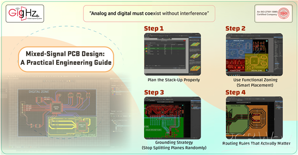
A correct stack-up is the foundation of signal integrity.
A typical 4-layer mixed-signal stack:
Layer 1: Signals
Layer 2: Solid Ground Plane
Layer 3: Power Plane
Layer 4: Signals
A continuous ground plane ensures controlled return current paths and reduces noise coupling.
Without a proper stack-up, signal integrity and EMI performance become unpredictable.
Component placement should follow functional grouping rather than random distribution.
Recommended zones:
Analog Section
ADCs
Op-amps
Sensors
Reference circuits
Digital Section
Microcontrollers
Memory devices
Clock circuits
Communication interfaces
Power Section
Switching regulators
Linear regulators
Filters
Keep each zone tightly grouped and avoid mixing functional blocks unnecessarily. Placement defines routing efficiency and noise behavior.
One of the most misunderstood areas in mixed-signal design is grounding.
In most modern PCB designs:
Use a single continuous ground plane
Avoid arbitrary ground splitting
Ensure short return paths for all signals
Splitting ground planes incorrectly can increase EMI and force return currents to take longer paths, degrading signal integrity.
The objective is not separation — it is controlled return current flow.
Routing discipline is one of the most critical factors in reliable PCB design.
Now let’s get practical.
Rule 1: Never Route Digital Signals Through Analog Zone
Digital signals carry fast edges.
Fast edges generate noise.
If routed near ADC inputs, they inject interference.
Keep digital routing inside digital zone.
Rule 2: Protect ADC Reference Lines
ADC reference is extremely sensitive.
Keep reference trace short
Avoid running it parallel to digital traces
Shield with ground where possible
Avoid vias if you can
A noisy reference = inaccurate measurement.
Rule 3: Keep Clock Lines Contained
Clock signals are strong noise sources.
Route them short
Avoid crossing analog sections
Avoid running them over plane splits
Surround with ground when possible
Treat clocks like controlled high-frequency signals.
Rule 4: Separate Analog and Digital Power
Even if ground is common, power should be filtered.
Use:
Ferrite beads between AVDD and DVDD
Separate decoupling networks
LC filters for analog rails
For example:
DVDD → Digital logic
AVDD → ADC + analog front end
Filtered properly.
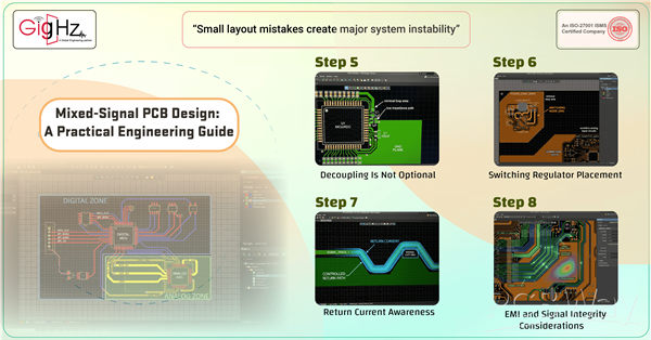
Decoupling capacitors are essential for stable operation.
Best practices:
Place capacitors as close as possible to IC power pins
Use short trace connections to ground
Combine multiple values (e.g., 100nF + 1µF)
Poor decoupling leads to noise coupling and voltage instability.
Switching regulators are major noise sources.
Guidelines:
Keep SMPS circuits physically isolated from analog sections
Minimize switching loop area
Avoid routing sensitive signals near inductors
Poor placement here can affect the entire analog subsystem.
Every signal follows a return path directly beneath its trace.
If a signal crosses a gap or splits in the ground plane:
Return current takes a longer path
Loop area increases
EMI levels rise
Maintaining a continuous reference plane is essential for predictable behavior.
Most EMI failures in mixed-signal designs come from:
Large loop areas
Broken return paths
Poor high-speed routing control
To reduce EMI:
Minimize loop areas
Maintain solid ground planes
Control trace impedance
Keep high-speed edges contained
Consider a system with:
100 MHz MCU
16-bit ADC
Temperature sensor
Switching regulator
Poor design results in:
SMPS near ADC
Clock routed across analog zone
Long reference traces
Split ground plane
Result: ADC noise variation ±15 LSB
Improved design:
Functional zoning applied
Solid ground plane maintained
Filtered analog supply
Short reference routing
Clock isolation
Result: Stable readings within ±1 LSB
Same components — different layout discipline.
Splitting ground planes incorrectly
Long analog signal paths
Clock routing near sensor inputs
Poor decoupling placement
Placing switching regulators near analog circuits
Routing over ground gaps
Most failures are predictable and preventable.
Before generating Gerbers:
Ground plane is continuous
Analog and digital zones are clearly separated
Clock lines are controlled and isolated
ADC reference routing is short
Decoupling capacitors are correctly placed
Switching regulators are isolated from analog circuits
If all conditions are met, the design is ready for fabrication.
Mixed-signal PCB design is not about physically separating analog and digital sections. It is about controlling electrical behavior across the entire board.
Successful designs focus on:
Return current control
Noise path management
Proper grounding strategy
Careful placement and routing discipline
Digital circuits generate noise.
Analog circuits measure signals.
PCB layout determines whether both works together or interfere with each other



