In electronic product development, hardware design, equipment maintenance, and PCB design, schematic diagrams serve as the essential bridge between design, manufacturing, and debugging. At the core of every schematic are circuit symbols, the fundamental building blocks that represent electronic components in a simplified and standardized visual form.
These electronic symbols allow engineers to quickly understand circuit structures, analyze signal flow, and implement accurate designs across the entire development workflow. Whether working on simple circuits or complex embedded systems, mastering schematic symbols is a key skill for every electronics engineer.
Circuit symbols are simplified graphical representations of electrical and electronic components used in schematic diagrams. Based on international and industry standards, these symbols communicate component functions, electrical connections, polarity, and signal flow while eliminating unnecessary physical details.
Instead of depicting the actual appearance of a resistor, capacitor, transistor, or integrated circuit, schematic symbols focus on the electrical characteristics that matter most during circuit design and analysis.
Although some symbols vary slightly between standards such as IEC and ANSI, their core meanings remain universally recognized. This standardization offers several important benefits:
Circuit symbols provide a universal engineering language that allows designers, manufacturers, and technicians worldwide to interpret the same schematic regardless of their native language.
Compared with text-based descriptions, schematic symbols make complex circuits easier to understand, especially in large designs containing hundreds or thousands of components.
Standardized symbols minimize interpretation mistakes throughout the entire workflow, from schematic capture and PCB layout to assembly and maintenance.
Today's ECAD software links circuit symbols directly with PCB footprints, 3D models, BOM data, and manufacturing files, enabling seamless integration between electrical and mechanical design.
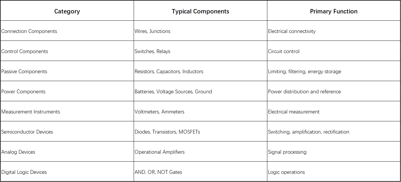
The table below summarizes the major categories of circuit symbols used in electronic design.
Most circuit symbols are not arbitrary drawings. They are simplified visual representations derived from a component's physical structure, operating principle, or electrical behavior.
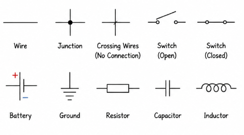
A straight line represents a conductor. Since a wire's primary function is simply to carry current, a simple line effectively reflects its role. Intersections marked with a dot indicate an electrical connection, while crossings without a dot represent non-connected conductors.
Switch symbols visually represent the opening and closing of electrical contacts, directly reflecting the two operating states of a circuit: connected and disconnected.
The familiar long and short parallel lines represent the positive and negative terminals of a battery, helping designers quickly identify polarity.
Additional rays extending from the symbol indicate the conversion of electrical energy into light.
For more advanced devices such as diodes, transistors, and operational amplifiers, the symbols emphasize current flow direction, control mechanisms, and terminal functions.
Based on their functions, electronic symbols can be divided into six major categories.
These symbols serve as the foundation of every circuit.
Straight lines represent conductors.
Dots indicate electrical connections.
Crossing lines without dots indicate no connection.
Various switch symbols represent push buttons, toggle switches, and selector switches. Relay symbols typically include both a coil and contact section, identifying normally open (NO) and normally closed (NC) contacts.
Passive components do not require external power for operation and cannot amplify signals.
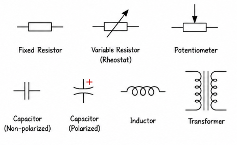
IEC standards commonly use rectangular resistor symbols, while ANSI standards use zigzag representations. Variable resistors include an arrow indicating adjustable resistance.
Primary applications include: Current limiting, Voltage division, Load matching.
Capacitor symbols consist of two parallel plates.
Polarized capacitors require correct orientation and are commonly used for: Power filtering, Energy storage.
Non-polarized capacitors are frequently used in high-frequency circuits.
Inductor symbols resemble coils of wire, reflecting their magnetic energy storage function.
Typical applications include: EMI suppression, Filtering, Energy storage.
Transformers are represented by two coupled coils and are used for voltage conversion and electrical isolation.
These symbols establish the electrical foundation of a circuit.
Battery symbols represent one or more electrochemical cells and indicate supply polarity.
Ground serves as the common voltage reference point and current return path.
Common types include: Signal Ground, Power Ground, Chassis Ground.
Power supply symbols are widely used in integrated circuits and digital systems.
Measurement symbols indicate proper connection methods during testing and debugging.
Represented by a circle containing the letter "A". Must be connected in series to measure current.
Represented by a circle containing the letter "V". Must be connected in parallel to measure voltage.
Semiconductors are among the most important components in modern electronics.
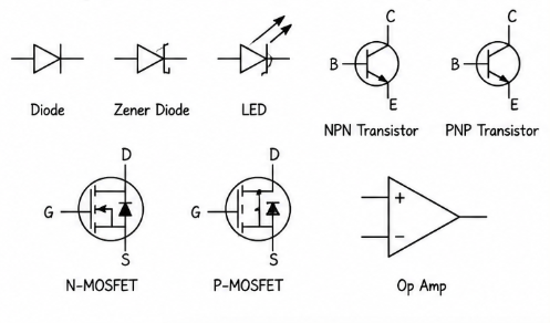
Basic diode symbols indicate one-way current conduction.
Common variants include: Rectifier Diodes, Zener Diodes, Light Emitting Diodes (LEDs), DIACs.
Bipolar Junction Transistors (BJTs): NPN and PNP transistors are distinguished by the emitter arrow direction.
MOSFETs: MOSFET symbols highlight the insulated gate structure and are widely used in switching and power applications.
SCR symbols include an additional control gate for high-power switching applications.
Operational amplifiers are represented by triangular symbols with differential inputs and a single output, making them essential building blocks for analog signal processing.
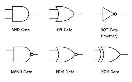
Logic gates form the foundation of digital electronics.
Common logic symbols include: AND Gate, OR Gate, NOT Gate, NAND Gate, NOR Gate, XOR Gate.
By combining these basic building blocks, engineers can create flip-flops, registers, processors, and complex digital systems.
Although most electronic symbols have universal meanings, slight visual differences exist between international standards.
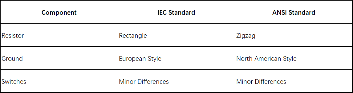
Modern ECAD software supports both standards. Understanding both systems improves collaboration across international engineering teams.
Many beginners view circuit symbols as simple drawings used only in schematics. In reality, they play a critical role throughout the entire PCB development process.
Circuit symbols define:
Every schematic symbol is linked to a corresponding PCB footprint.
The software transfers netlist information from the schematic to the PCB layout based on this symbol-to-footprint relationship.
Incorrect pin assignments can lead to routing errors, malfunctioning hardware, or even component damage.
Symbol data contributes directly to:
Well-maintained component libraries significantly reduce manufacturing risks.
Engineers rely heavily on schematic diagrams during troubleshooting and repair. Clear, standardized symbols make fault isolation faster and more efficient.
It is important to note that circuit symbols define only the electrical logic of a design. Final product performance depends heavily on PCB layout quality, including routing strategy, grounding architecture, signal integrity, and power integrity considerations. You can read this article to learn more about the PCB Layout: PCB Layout Design Guide
Standard component libraries cannot cover every device used in modern hardware development. Custom ICs, proprietary modules, and specialized connectors often require custom schematic symbols.
A typical workflow includes:
Circuit symbols are the universal language of electronics, enabling engineers to communicate circuit functionality, signal flow, and design intent through standardized graphical representations. From basic components such as resistors and capacitors to complex semiconductor devices and logic circuits, understanding schematic symbols is an essential skill for circuit design, PCB development, troubleshooting, and manufacturing.
As electronic products become increasingly sophisticated, accurate symbol creation and library management play a critical role in ensuring design quality and reducing development risks. PCBWay Design Service provides professional support for schematic design, custom symbol and footprint creation, PCB layout, DFM review, and enclosure design, helping transform ideas into reliable, manufacturable products more efficiently.


