Many high-speed PCBs appear correct during schematic design, yet after fabrication, problems such as FPGA configuration failures, unstable DDR timing, ADC noise, EMC radiation issues, and excessive power ripple may still occur. In many cases, the root cause is not the IC itself, but improper decoupling capacitor design.
With extensive experience in high-speed PCB design and layout optimization, PCBWay Design Service has summarized practical decoupling capacitor placement guidelines covering capacitor selection, PCB stackup, placement strategy, and PDN optimization to help engineers improve power integrity and overall system stability.
Understanding Decoupling and Bypass Capacitors
Decoupling Capacitor vs Bypass Capacitor
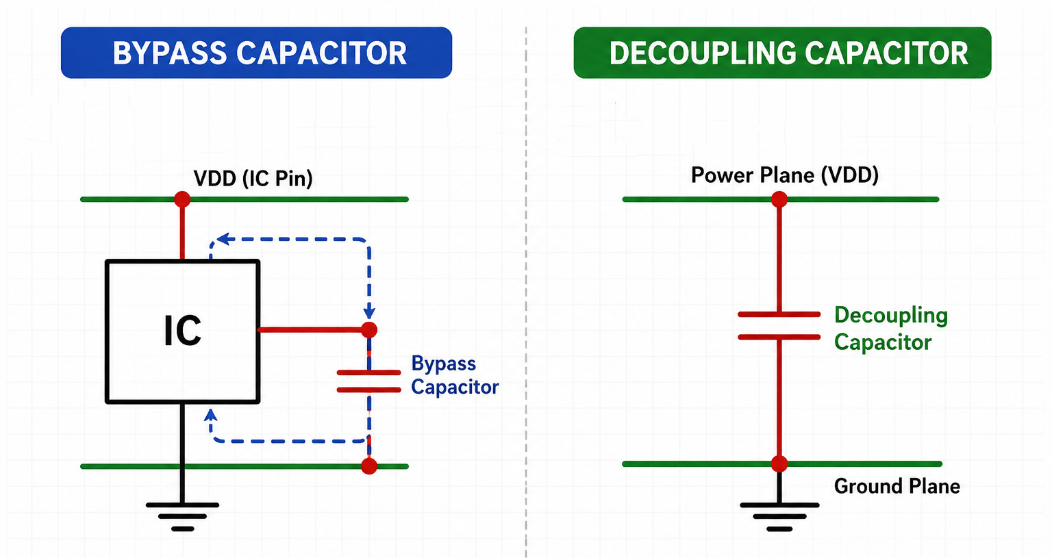
Although the terms are often used interchangeably, decoupling capacitors and bypass capacitors serve different purposes in power integrity design.
- Bypass Capacitor: Connected directly between an IC power pin and ground, mainly used to suppress high-frequency noise and reduce ground bounce. During switching events, the bypass capacitor provides local transient current and prevents high-frequency noise from spreading through the power rail.
- Decoupling Capacitor: Connected between the power plane and ground plane, mainly used to stabilize the PDN, compensate for low-frequency fluctuations, and reduce coupling between different functional blocks sharing the same power network.
In simple terms: Bypass capacitors stabilize local high-frequency switching current. Decoupling capacitors stabilize the overall board-level power network. Together, they form the foundation of PCB power integrity.
Why Decoupling Capacitors Stabilize Voltage
High-speed ICs such as FPGAs, CPUs, and RF chips generate transient current spikes within nanoseconds during switching events. PCB traces and vias contain parasitic inductance, and the impedance increases with frequency: Z=2πfL. As current changes rapidly, voltage drops occur at the power pins, potentially causing logic instability or timing errors.
A decoupling capacitor acts as a local energy reservoir:
- storing charge during steady-state operation,
- rapidly discharging during transient current demand,
- and recharging after the switching event ends.
The primary goal of decoupling capacitor placement in PCB design is therefore: minimizing the high-frequency current loop area and reducing transient voltage drop.
ESR, ESL, and SRF: Key Parameters in High-Speed PCB Design
Real capacitors are not ideal components. Their high-frequency performance is determined by three critical parasitic parameters:
- ESL(Equivalent Series Inductance): Introduced by capacitor packages, PCB pads, routing, and vias. Higher frequency means higher ESL impedance, making it more difficult for the capacitor to deliver transient current.
- SRF(Self-Resonant Frequency): The frequency where capacitive reactance equals inductive reactance. Below SRF, the capacitor behaves capacitively and filters noise normally. Above SRF, it becomes inductive and may even amplify noise.
- ESR(Equivalent Series Resistance): Affects charge and discharge speed. Excessively low ESR may cause PDN resonance, while excessively high ESR weakens transient response capability.
Decoupling Capacitor Selection Guidelines
The core principle of capacitor selection is straightforward: capacitor value, package, and material must match the operating frequency range and transient current demand of the system.
Multi-Stage Decoupling Structure for Wide Frequency Coverage
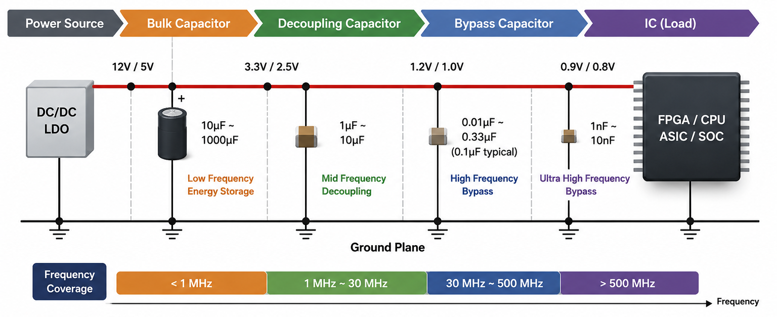
High-speed systems contain noise spanning from kHz to GHz frequencies. Therefore, multiple capacitor stages are required.
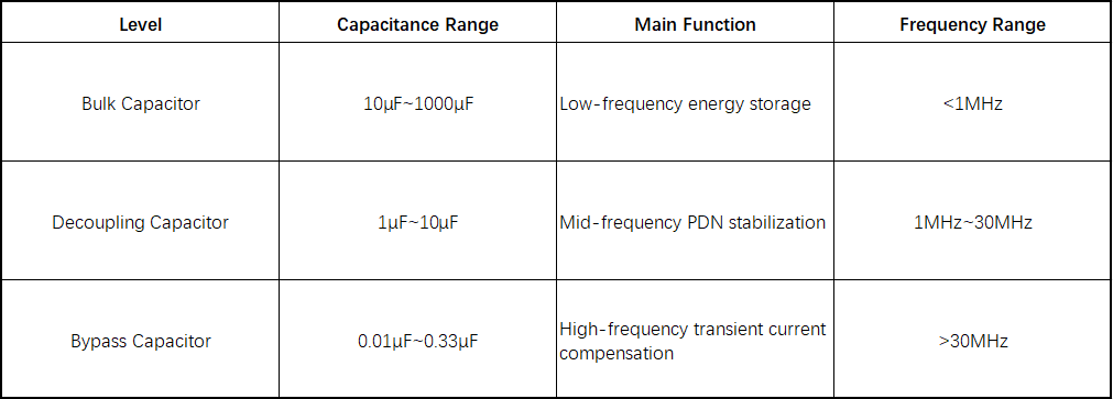
For DDR5, high-speed SerDes, and RF systems, additional 1nF~10nF ultra-low ESL capacitors are often required for GHz-frequency suppression.
Capacitor Material and Package Selection
Capacitor Material
- High-frequency applications (>100MHz): NPO/COG capacitors are preferred due to low ESL and high SRF.
- Mid- and low-frequency applications: X7R and X5R are widely used.
- Bulk energy storage: Solid tantalum and aluminum electrolytic capacitors are commonly used.
Capacitor Package Selection
In high-speed PCB design: smaller capacitor packages generally provide lower ESL.
Typical recommendations:
- 0201 and 0402 for high-frequency systems,
- 0603 and 0805 for general-purpose applications.
For GHz-frequency systems, package size is often more important than increasing capacitance.
Critical Parameter Verification
- Voltage Margin: The capacitor voltage rating should be at least: Vrated≥1.5×Vworking to avoid voltage overstress.
- SRF MatchingL: The SRF should remain above the target noise frequency range to maintain capacitive behavior.
- PDN Target Impedance: PDN target impedance can be estimated using: Ztarget=ΔV÷ΔI. Matching ESR to the target impedance helps prevent excessive PDN resonance.
PCB Decoupling Capacitor Placement Guidelines and Stackup Optimization
The essence of decoupling capacitor placement guidelines is simple: minimize loop inductance and high-frequency current path length. Different PCB stackups require different placement strategies.
General Decoupling Capacitor Placement Guidelines
- Local bypass capacitors should be placed as close as possible to IC power pins.
- Capacitors should connect directly to power and ground planes whenever possible.
- Long routing between capacitors and ICs should be avoided.
- Short vias or Via-in-Pad structures are recommended.
- Different power rails should use independent decoupling networks.
Decoupling Capacitor Placement for Two-Layer PCBs
Two-layer PCBs do not have solid power and ground planes, resulting in higher parasitic inductance. Therefore, the current loop must be minimized aggressively:
- Each IC should include a local 0.01μF~0.1μF capacitor.
- 10μF~100μF bulk capacitors should be added near the power input.
- Capacitors should be placed directly adjacent to the IC whenever possible.
Decoupling Capacitor Placement for Multi-Layer PCBs
For 8-layer to 14-layer high-speed PCBs:
- power and ground planes are closely spaced,
- plane capacitance increases,
- and high-frequency return paths become more stable.
Recommended techniques include:
- using multiple capacitors of the same value in parallel,
- implementing Via-in-Pad structures,
- placing capacitors within the effective energy circle of the IC.
Decoupling Capacitor Placement for Four-Layer PCBs
Typical 4-layer PCBs often have relatively large spacing between power and ground planes, which weakens high-frequency performance.
Therefore:
- capacitors must remain on the same side as the IC,
- capacitors must stay extremely close to power pins,
- and power/ground vias should be tightly paired.
Otherwise, loop inductance increases significantly.
BGA and High-Speed Package Decoupling Design
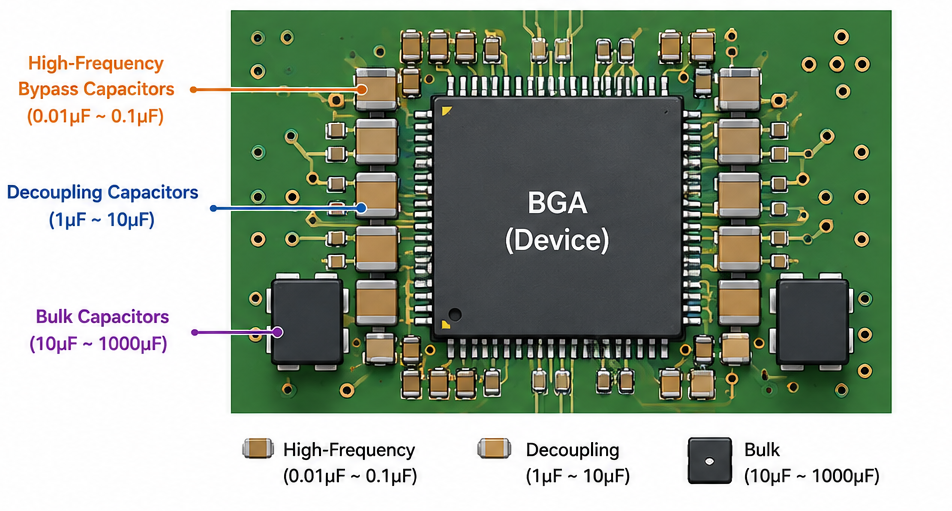
BGA, FPGA, and CPU devices require specialized decoupling capacitor placement because of dense pin structures and complex fanout routing:
- Via-in-Pad structures should be prioritized.
- Backside decoupling should be used where appropriate.
- Shared via structures and fanout routing should be optimized.
- The distance between BGA power pins and decoupling capacitors should be minimized.
These details directly affect PI, SI, and EMI performance.
Common Decoupling Design Mistakes
- Using only 0.1μF capacitors everywhere: Different systems require different frequency coverage. High-speed systems often require 0.1μF, 10nF, and 1nF capacitors working together.
- Placing decoupling capacitors too far from the IC: Extra routing and via length significantly increase ESL and weaken transient response performance.
- Blindly mixing different capacitor values: Different SRFs may create anti-resonance, causing PDN impedance spikes and amplified noise.
PI/PDN Simulation and Validation
High-speed PCB decoupling design should always be verified through simulation and measurement, including:
- PDN impedance scanning
- Power ripple measurement
- EMI/EMC pre-compliance testing
- Transient response analysis
Simulation and measurement help identify:
- resonance peaks,
- abnormal high-frequency impedance,
- return path discontinuities,
- and EMC risks
before mass production, significantly reducing debugging cost.
In high-speed digital, mixed-signal, and RF PCB projects, proper decoupling capacitor placement often directly determines system stability and EMC performance. For complex high-speed PCB designs, decoupling strategies should also be coordinated with PI/SI analysis, stackup optimization, and manufacturing constraints.
PCBWay provides professional PCB Design, High-Speed PCB Layout, SI/PI Optimization, and Manufacturing-Ready Engineering Services to help engineering teams reduce EMI risks, improve system stability, and accelerate product development from design to production.



