In DCDC power design, the circuit defines the function, but PCB layout determines success or failure. Even with correct component selection and accurate calculations, issues such as audible noise, overheating, excessive ripple, or EMC failure may still occur. In reality, over 90% of these problems originate from poor PCB layout rather than the circuit itself.
This article summarizes practical, experience-driven guidelines for power PCB layout, helping improve stability, reduce debugging time, and achieve first-pass success.
Core Principles: 3 Rules of DCDC Layout
A DCDC converter operates through high-frequency switching: input voltage → PWM control → power switching → energy storage in the inductor → regulated output.
The effectiveness of any pcb layout for power supply design depends on three key principles:
- Power Loop: High current and high di/dt paths must be short, wide, and compact to minimize loop area, parasitics, and EMI
- Feedback Path: Sensitive analog signals must be clean and isolated from noise sources to ensure accuracy
- Ground System: Separate power ground and signal ground, then connect at a single point
In short: minimize the power loop, keep signals clean, and control the ground path.
Start with the Datasheet
One of the most common mistakes in layout pcb power supply design is skipping the datasheet and starting layout immediately.
A correct workflow includes:
- Review the chip’s recommended layout
- Follow placement guidelines for: Input capacitors, Inductor, Ground connections, Thermal pads
- Prioritize placement of the power loop and critical pins
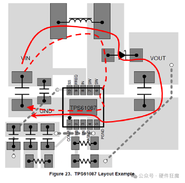
The reference layout provided by manufacturers is already optimized and verified—use it as your starting point.
Placement: Compact and Clear
A good layout pcb power design ensures a clear current flow:
- Place components around the IC as the center
- Arrange the flow in sequence: input → power stage → output
- Keep input and output filtering physically separated to avoid noise coupling
Power Loop: Keep It Small
Main current path: Input → Input Capacitor → IC → Inductor → Output Capacitor → Load
Key practices:
- Avoid unnecessary vias or layer transitions
- Keep traces short and direct
- Place input capacitors close to Vin and PGND (preferably < 40 mil)
- Minimize parasitic inductance through tight placement
A smaller loop means lower EMI, higher efficiency, and better thermal performance.
Routing: Short, Wide, Direct
High Current: Use Copper
- Use large copper areas for power and ground whenever possible
- Increase trace width if copper pour is not feasible
- Avoid narrow traces for high current paths
- Minimize copper area at the SW node (a major noise source)
Signals: Stay Clean
- Trace width ≥ 10 mil (or match pad size)
- Avoid 90° corners; use 45° or rounded routing
- Keep signal traces away from switching nodes and power loops
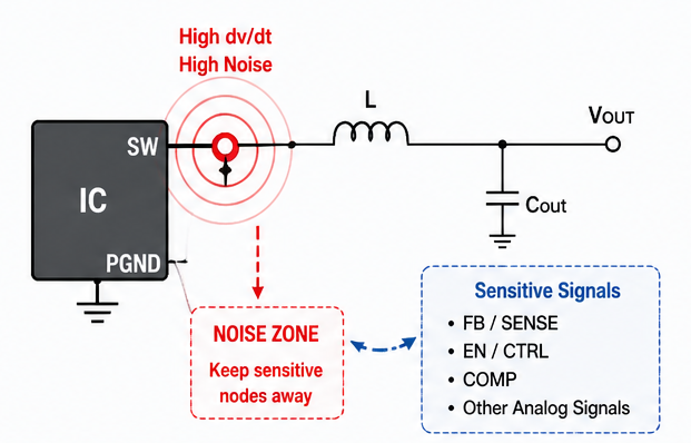
Critical Pins: Don’t Get Them Wrong
Improper handling of key pins often leads to instability, noise, or regulation errors in pcb layout for power supply.
FB/SENSE: Accurate Sampling
- Sense voltage from the output capacitor
- Avoid routing through power paths
- Keep traces isolated from switching noise
GATE: Stable Drive
- Use short and wide traces
- Avoid interference from noisy regions
- Reduce switching losses and ringing
INTVCC: Close Decoupling
- Place decoupling capacitors close to the pin
- Ensure stable gate driver supply
Ground & Thermal: Build the Foundation
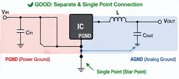
Grounding: Separate then Join
- PGND (Power Ground): High current path with wide copper and multiple vias
- AGND (Analog Ground): Clean reference for sensitive signals
- Connect them at a single point near the IC
Keep-Out Areas
- Under the IC: Only ground plane and thermal vias
- Under the inductor: No signal routing to avoid magnetic coupling
Thermal: Use Vias
- Use via arrays under PowerPAD for heat dissipation
- Open solder mask for better thermal transfer
- Add vias in high-current regions to improve conductivity and cooling
Advanced Tips for Power PCB Layout
- Place inductors in multi-channel designs perpendicular to reduce coupling
- Use thermal relief (cross connections) for pads connected to large copper
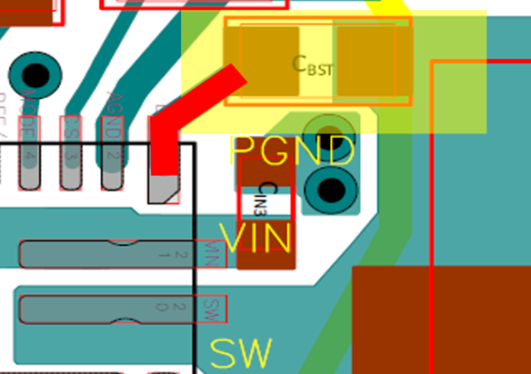
- Keep BST capacitor close to BST and SW pins, with wide traces
Conclusion
Effective layout pcb power supply design is about balancing electrical performance, EMI control, and thermal management. A well-optimized power pcb layout not only improves system stability but also significantly reduces debugging time and redesign costs.
PCBWay design service leverages extensive experience in power supply design to optimize layout pcb power solutions, identify potential risks early, and improve first-pass success rates—helping projects move efficiently toward mass production.


