PDN (Power Distribution Network) is a critical part of PCB design, directly determining power delivery efficiency, noise suppression capability, and overall system stability. Skipping PDN simulation and rushing into fabrication often leads to severe issues such as startup failure, system crashes, or even power damage. In the 5G era, especially with the widespread adoption of POP packaging—where DDR routing is embedded inside the package—PDN design has become a mandatory checkpoint for advanced HDI boards.
In this article, the PCBWay design team shares practical engineering experience and summarizes essential PDN design guidelines to help designers successfully optimize their PDN implementation.
Capacitors play a vital role in PDN design, particularly in noise suppression and voltage stabilization. The four types—coupling, filtering, decoupling, and bypass capacitors—have distinct functions, and misuse can significantly affect PDN simulation results.
1. Coupling Capacitors
These are the only capacitors connected in series, used to block DC and pass AC signals (e.g., AC coupling in high-speed SERDES). They have minimal impact on PDN design and are typically ignored in PDN simulations.
2. Filtering Capacitors (Bulk Capacitors)
Connected in parallel at power input/output, they stabilize the power supply by filtering low-frequency ripple and noise. Common values include 47µF–100µF electrolytic or tantalum capacitors. These are essential in PDN design guidelines for low-frequency stability.
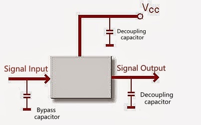
3. Decoupling Capacitors
Positioned from the load perspective, they suppress noise generated by ICs and reduce interaction between loads. Often used with ferrite beads or resistors, they are crucial for mid-to-high frequency noise control in PDN design.
4. Bypass Capacitors
Focused on high-frequency noise suppression, they provide a low-impedance path to ground. Typically small-value (pF/nF) and small-package (0201/01005), they must be placed very close to IC power pins—one of the most important PDN design guidelines.
Filtering capacitors stabilize the power source, decoupling capacitors protect loads, bypass capacitors handle high-frequency noise near pins, and coupling capacitors belong to signal paths. PDN design optimization mainly focuses on filtering, decoupling, and bypass capacitors.
1. Bypass Capacitors Becoming Ineffective
When bypass capacitors are placed on a different layer from the IC, they can be unintentionally bypassed. For example, if the IC is on the bottom layer and the capacitor is on the top, the power may flow directly through internal layers to the IC, completely skipping the capacitor.
PDN Design Guidelines:
2. Missing Ground (GND) Path Matching
Ground is an inseparable part of PDN design, acting as the return path. A common mistake is aligning only the power pad while ignoring the GND pad, relying on surface copper instead. This increases loop inductance and weakens high-frequency performance.
PDN Design Guidelines:
3. Component Size vs. Placement Density Conflict
In consumer electronics, ultra-small packages (e.g., 01005) allow dense capacitor placement. However, automotive or industrial designs often require 0402 or larger packages, reducing capacitor count within the same area and making PDN design optimization harder.
PDN Design Guidelines:
4. Power/Ground Plane and Return Path Issues
Common problems include:
Narrow power traces or incomplete ground planes → high impedance and voltage drop
Split planes under high-speed signals → longer return paths and increased EMI
Poor isolation between power domains → noise coupling
PDN Design Guidelines:
Ignore coupling capacitors in PDN simulation; use bulk capacitors for low frequency, and combine multiple values of bypass/decoupling capacitors near IC pins to cover a wide frequency range.
Keep bypass capacitors on the same side as ICs, align GND pads precisely, and use pad optimization techniques to increase capacitor count. Embedded capacitance is an advanced solution for high-end PDN design.
Ensure power paths are short, wide, and direct; maintain continuous ground planes; match via count to current requirements; and minimize return path length.
Always perform PDN simulation before fabrication. Validate impedance, ripple, and voltage drop to ensure compliance with PDN design guidelines.
Effective PDN design is fundamentally about achieving low impedance, short current paths, strong noise filtering, and stable return paths. In advanced HDI and high-speed 5G applications, following these PDN design guidelines can significantly improve first-pass success rates and ensure reliable system performance.
If you need support with your PDN design, the PCBWay design team can provide professional guidance based on extensive engineering experience to help you achieve a robust and production-ready solution.