Once the PCB stack-up is defined, nearly 80% of the total manufacturing cost is effectively locked in. This is especially true for HDI PCB design, where stack-up decisions directly determine the build-up structure, microvia configuration, and overall process complexity.
Stack-up selection should always start from routing requirements, rather than being constrained by manufacturing considerations too early. There is no need to select a high-level HDI structure at the beginning. While it may seem “safer,” the cost will increase rapidly. The stack-up only needs to meet the actual design requirements—nothing more.
At the design stage, the first step is to determine the minimum HDI level required to complete routing. This decision should be based on the following key factors:
Practical examples:
This is the starting point of requirement analysis. The following aspects should be clearly defined to determine whether HDI is required and how many build-up layers may be needed:
After determining routing density, evaluate whether BGA fan-out is feasible:
If fan-out can be completed at a lower HDI level, a simpler structure should always be preferred.
Based on the conclusions from the previous steps, select the simplest and most cost-effective structure that meets the requirements. Performance only needs to meet design targets—overdesign should be avoided.
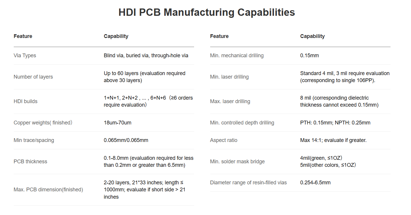
Once the stack-up is defined, it should be confirmed with the HDI PCB manufacturer to ensure feasibility. Early DFM verification during the design stage helps avoid redesigns, board revisions, and mass-production risks. You can consult PCBWay regarding manufacturing capabilities to assist in completing your HDI design.
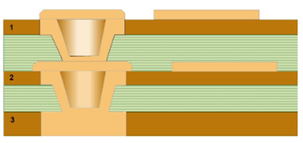
Staggered microvias are offset between adjacent layers rather than aligned vertically. This structure distributes stress more evenly during thermal expansion or board bending. For applications with high reliability requirements or frequent thermal cycling, staggered microvias should be prioritized.
Excessive aspect ratios make it difficult for plating solutions to uniformly coat the via walls, leading to uneven copper thickness or voids. This severely impacts both electrical reliability and mechanical strength. Proper dielectric thickness and build-up planning are essential to keep microvia aspect ratios within a stable manufacturing window.
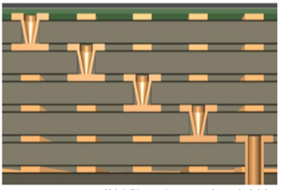
As the number of stacked vias increases, accumulated stress concentration and CTE mismatch risks rise sharply, and failure probability increases exponentially. Stacked vias should therefore be minimized whenever possible.
Asymmetrical stack-ups can introduce uneven stress during lamination, increasing the risk of warpage. This affects both manufacturability and long-term reliability. In high-speed or high-current areas, build-up layer placement should be planned by balancing electrical performance and mechanical reliability
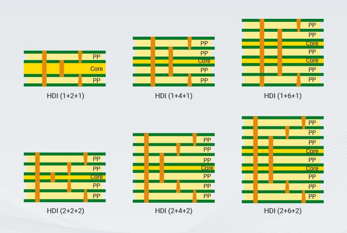
Each lamination cycle is a complete manufacturing process involving lamination, drilling, and plating. The HDI “order” (1st order, 2nd order, or any-layer) directly determines the minimum number of lamination cycles required. Every additional cycle increases lead time, material consumption, and yield loss risk. Lamination count is one of the most significant cost drivers in HDI PCB fabrication.
Via-in-pad requires additional resin filling and planarization processes, with extremely high requirements for precision and materials. This significantly increases manufacturing cost and should only be used when absolutely necessary.
Selecting any-layer HDI at the initial design stage purely for safety often results in a dramatic cost increase. Designers should always start with the lowest-cost structure and only upgrade when core routing requirements cannot be met.
Designs that are not verified with the manufacturer may turn out to be unbuildable, requiring major redesigns. After defining a preliminary stack-up, it is essential to communicate with the PCBWay factory to ensure manufacturability.
Focusing only on electrical performance while using excessive stacked vias can lead to severe stress concentration due to CTE mismatch between materials. This often causes copper cracking or delamination. Designers should prioritize staggered vias over vertically stacked vias and proactively add thermal vias in high-power areas to distribute and dissipate heat.
The core of HDI lamination design is to achieve an optimal balance between performance, reliability, and cost. Designers should focus on realizing product functionality through the simplest and most manufacturable structures possible. By controlling complexity at the lamination stage, HDI PCB designs can significantly improve manufacturing yield, reduce production risks, and ensure long-term product stability.
Feel free to ask PCBWay HDI Manufacturer to help your design be better!


