In many hardware projects, schematic design is often underestimated. Engineers move into PCB layout before fully defining circuit logic, signal flow, and design constraints, which can lead to multiple board re-spins, difficult debugging, and even production risks.
In reality, a well-executed pcb schematic design can eliminate up to 80% of potential issues at an early stage. A schematic is not just a wiring diagram—it is a unified carrier of circuit logic, signal flow, manufacturing constraints, and team collaboration.
This article presents a practical and structured approach to pcb schematic design based on four key dimensions: modular hierarchy, standardization, intelligent verification, and production readiness—combining real-world experience from PCBWay design team.
The Importance of Schematic Design
The role of a schematic goes far beyond connectivity. A high-quality pcb schematic design delivers value across four key layers:
- Logical Layer: Ensures functional correctness and proper electrical connections
- Standardization Layer: Unifies symbols, reference designators, and network structures for readability
- Engineering Layer: Prepares the design for PCB layout, SI/PI performance, and EMC compliance
- Collaboration Layer: Enables efficient review, version control, BOM generation, and manufacturing alignment
Key Elements of PCB Schematic Design
A complete and production-ready pcb schematic design must include the following core elements:
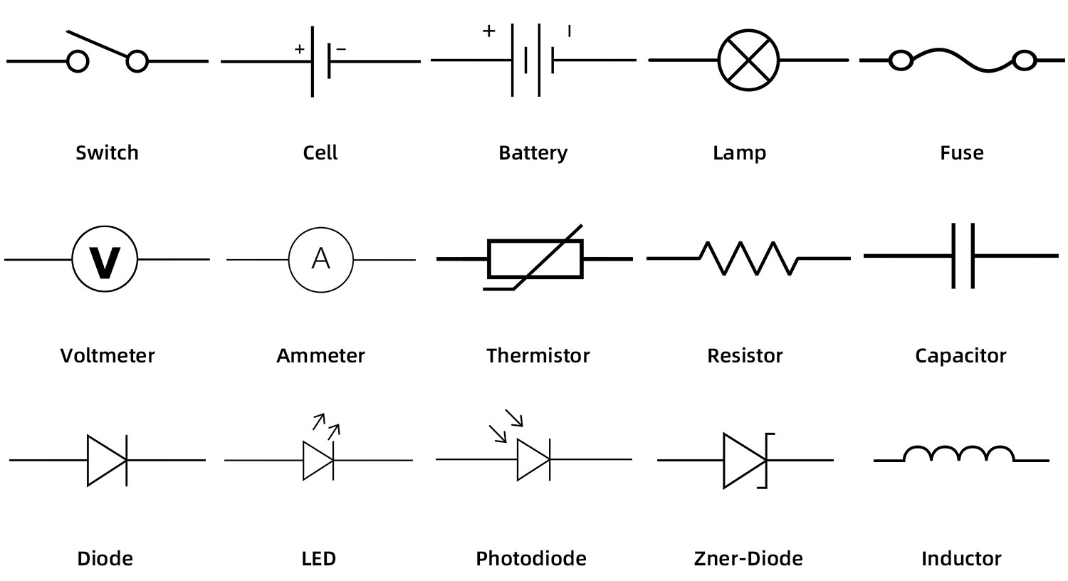
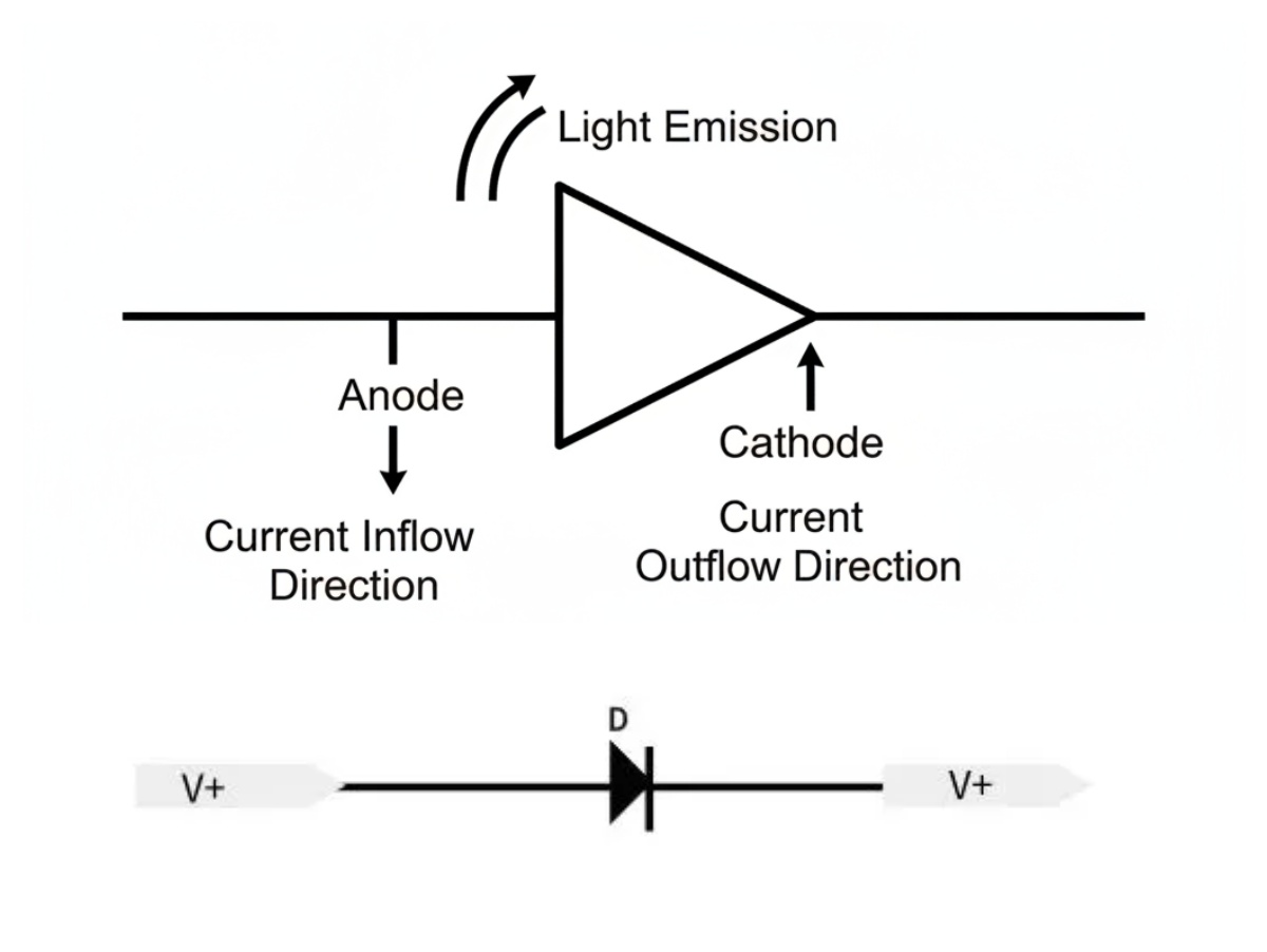
- Component Symbols: Represent electronic components such as resistors, capacitors, ICs, and connectors; standardized library symbols should be used to avoid ambiguity.
- Reference Designators: Unique identifiers (R, C, U, D, J, etc.) assigned to each component, ensuring consistency across schematic, BOM, and PCB for traceability.
- Electrical Connections: Define logical connectivity between components rather than physical routing; clean and structured connections improve readability.
- Power and Ground Networks: Clearly define different voltage rails and grounding types (e.g., +3.3V, +1.8V, AGND, DGND); proper segmentation is critical for noise control.
- Net Labels and Off-Page Connections: Enable cross-page connectivity while maintaining clarity; identical net names must represent the same electrical potential.
- Annotations and Parameters: Include component values, ratings, and design intent (e.g., pull-up/down, differential pairs), supporting debugging and manufacturing.
- Design Constraints: Define requirements such as impedance control, decoupling, signal integrity, and safety spacing to guide downstream design.
These elements ensure a smooth transition when moving from pcb schematic design to building a reliable pcb from schematic.
Standard PCB Schematic Design Workflow
1. Requirement Definition and System Architecture
- Define voltage, current, interfaces, speed, environment, and safety requirements
- Partition system into modules: power → analog/digital/RF → interface → control → storage
- Plan schematic pages by function
- Output: system block diagram, power tree, and signal flow diagram
This step ensures alignment before schematic entry and reduces rework when generating the pcb from schematic.
2. Component Selection and Library Management
- Use standardized libraries; custom symbols must follow clear orientation rules
- Split complex devices into functional units (e.g., U1A/U1B)
- Ensure reference designators follow IEEE naming conventions
- Clearly mark polarity-sensitive components
Standardization here directly improves the reliability of the pcb schematic design.
3. Hierarchical and Modular Schematic Design
3.1 Power Planning First
- Build a power tree: input → protection → regulation → load
- Define current requirements and noise sensitivity
- Separate analog, digital, and RF power domains
- Place decoupling capacitors close to IC pins
- Use clear naming conventions (e.g., +3V3_DIG, AGND)
3.2 Signal Flow (Left to Right)
- Maintain a consistent flow: input → processing → control → output
- Group buses and identify differential pairs
- Keep oscillators and matching circuits close to related components
3.3 Connectivity and Net Naming
- Avoid unnecessary wire crossings
- Use clear and short net names (≤8 characters)
- Mark active-low signals (~RESET, CS#)
- Standardize power and ground naming
A well-structured pcb schematic design ensures that the transition to pcb from schematic is smooth and error-free.
4. Power Integrity and Grounding Strategy
- Define complete power paths based on the power tree
- Separate ground domains using star or single-point grounding
- Ensure proper decoupling for each IC
Good power design at the schematic stage is essential for building a stable pcb from schematic.
5. Intelligent Electrical Verification
A multi-level verification process ensures design correctness:
- ERC Check: Detect opens, shorts, duplicate references, floating pins
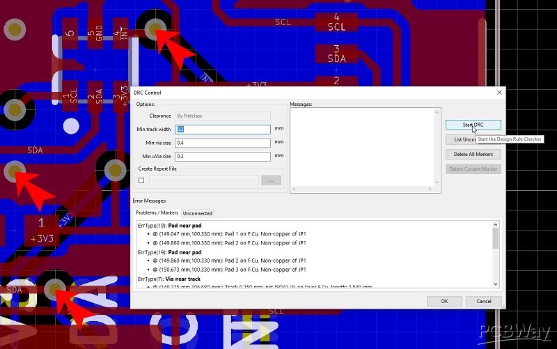
- DRC & Consistency Check: Verify symbol-to-footprint mapping and polarity. DRC tools can be used to automate validation. PCBWay DRC tools support across multiple EDA platforms, including KiCad, Altium Designer, EAGLE, and Allegro, allowing engineers to perform comprehensive checks using their preferred design environment.
- Manufacturing Check: Ensure BOM completeness, solderability, and safety compliance. You can check PCBWay’s manufacturing capabilities to confirm your schematic design.
- SI/PI Pre-check: Evaluate signal return paths, impedance, and crosstalk risks
These checks significantly improve first-pass success when converting pcb schematic design into a physical pcb from schematic.
6. Documentation and Review
- Improve layout readability and add design notes
- Organize schematic pages and index
- Maintain version history (date, author, changes)
- Verify cross-page connectivity
Clear documentation reduces communication cost across teams.
7. Output and Handoff
Deliverables should include:
- Schematic PDF
- System block diagram
- Power tree
- Netlist
- Complete BOM
- Version history
- Design constraints
These outputs ensure that every stakeholder can efficiently work on the pcb from schematic process.
Schematic Design Checklist
✅️ Is signal flow clear (left to right)?
✅️ Are power domains properly defined?
✅️ Are all critical nets labeled?
✅️ Are polarity-sensitive components correctly marked?
✅️ Are off-page connections consistent?
✅️ Have ERC/DRC checks been completed?
Common Mistakes to Avoid
❌️ Focusing only on connections instead of signal flow: Overlooking signal flow and functional partitioning leads to cluttered schematics, making debugging and maintenance significantly more difficult.
❌️ Poor power and ground design causing noise issues: Failing to separate analog and digital grounds or clearly define power domains can introduce noise coupling and cause unstable circuit behavior in the final PCB from schematic.
❌️ Missing annotations leading to manufacturing errors: Lack of component values and design constraints can result in procurement errors, manufacturing issues, and difficulties in troubleshooting.
❌️ Skipping validation checks: Not performing ERC/DRC checks may leave open circuits, short circuits, or floating pins undetected, allowing flawed designs to proceed into PCB layout.
❌️ Incorrect cross-page connections: Inconsistent net labeling or missing off-page connectors can lead to incorrect netlist generation and connectivity errors when creating the pcb from schematic.
❌️ Using inconsistent or incorrect component libraries: Using non-standard symbols or mismatched pin definitions may cause functional failures, even if the pcb schematic design appears correct.
Conclusion
A schematic is not just the starting point—it is the foundation that determines the success of the entire hardware development process. A well-structured pcb schematic design significantly reduces development risks and accelerates the transition to a production-ready pcb from schematic.
With extensive engineering experience, PCBWay design service helps identify potential issues at the schematic stage, optimize system architecture, and improve first-pass success rate—ensuring a smoother transition from design to mass production.


