During hardware development, failing EMC tests is a common issue. Many engineers try fixes such as adding shielding enclosures, replacing chips, or increasing capacitance. However, these approaches often fail to address the root cause and instead increase design cost. In reality, around 90% of EMC issues stem from improper grounding design.
Grounding is not just about connecting wires—it is a critical part of return path design and noise control in a circuit system, directly determining electromagnetic compatibility performance. A well-thought-out EMC PCB layout is essential to achieving reliable results.
Issue: To isolate digital ground, analog ground, and power ground, designers split the ground plane into multiple isolated regions. This creates discontinuities, forcing signal traces to cross gaps. As a result, return paths are extended, forming large loop areas and causing excessive EMI radiation.
Recommendation: Prioritize maintaining a continuous ground plane. Avoid splitting whenever possible. If splitting is necessary due to functional requirements, ensure that signal traces do not cross the gaps. Use ferrite beads or 0Ω resistors to connect split regions, providing a return path for high-frequency currents. This is a key practice in optimizing EMC in PCB design.
Issue: Ground traces are often treated casually—too thin, too long, or connected in series—under the assumption that “as long as it’s grounded, it’s fine.” This leads to voltage drops along the ground path, causing ground potential differences. The result can be ground bounce, MCU resets, reduced ADC accuracy, and unstable communication.
Recommendation: Use a solid ground plane whenever possible. If ground traces must be used, their width should be at least three times that of signal traces. Critical components should have their ground pins directly connected to the main ground plane through vias. This approach significantly improves overall EMC layout performance.
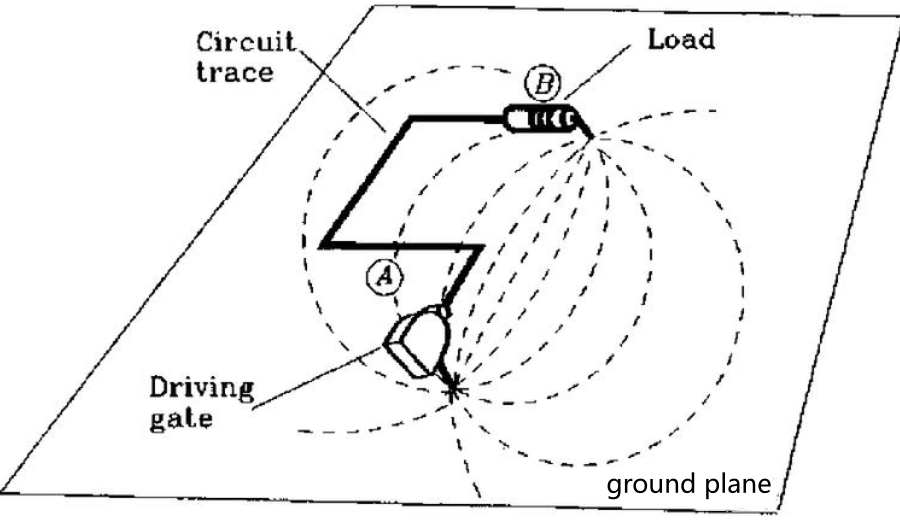
Issue: Designers often focus only on signal routing while ignoring the return path. Even if the forward signal path is short, the return current may be forced to detour, forming large loop areas that significantly increase EMI radiation.
Recommendation: Ensure that high-speed signal traces have a continuous ground plane directly beneath them to provide a proper return path. When signals change layers, place a ground via close to the signal via to maintain a short return path. During layout, always consider current flow and avoid crossing or overlapping return paths. This is fundamental to effective EMC PCB layout.
The primary purpose of grounding is to provide a low-impedance return path. In low-frequency circuits, resistance is the main concern; In high-frequency circuits, inductance dominates. A continuous ground plane minimizes high-frequency inductive impedance and is far superior to traditional ground traces—making it essential for EMC in PCB design.
The length of the return path directly affects loop area. The smaller the loop area, the lower the EMI radiation. Return paths should stay as close as possible to the signal traces to minimize loop size—this is one of the most effective EMC optimization techniques.
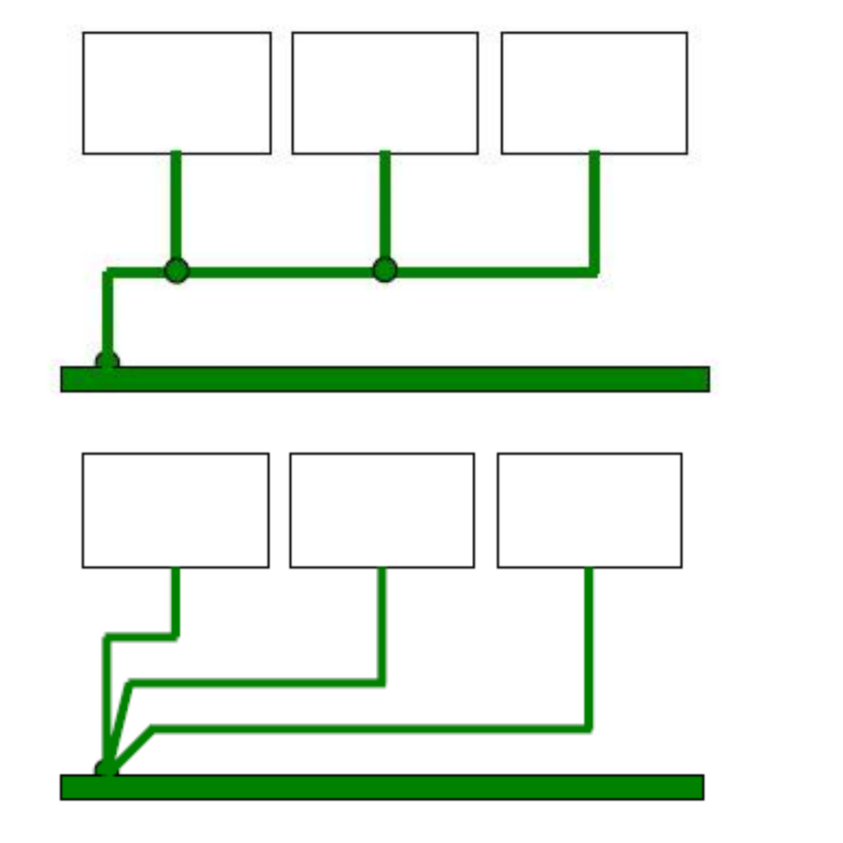
Low-frequency circuits (<1 MHz): Use single-point grounding to avoid ground loops.
High-frequency circuits (>10 MHz): Use multi-point grounding to reduce impedance.
Mixed-signal circuits: Use partitioning, with digital and analog grounds connected at a single point near the power entry to isolate noise.
Ground plane splitting is a double-edged sword. Proper implementation can isolate noise, but improper splitting disrupts return paths and creates EMC issues. Follow the principle: avoid splitting unless absolutely necessary. If splitting is required, strictly control signal routing and never allow traces to cross gaps.
In EMC design, grounding is not a detail to be fixed later, but a fundamental part of the PCB layout from the very beginning. By focusing on low-impedance return paths and maintaining a continuous ground reference, most EMC issues can be avoided before they arise.
In practice, achieving a robust EMC PCB layout often relies on accumulated design experience and careful trade-offs. The PCBWay design team has summarized these practical considerations through real-world projects, helping engineers optimize grounding strategies and improve overall EMC performance more efficiently.