In power supply design, linear regulators (LDOs) are widely used in portable devices, industrial control systems, and consumer electronics due to their simple circuitry, low ripple, and fast transient response. However, LDOs inherently suffer from power dissipation and thermal limitations. If not properly designed, they can reduce efficiency, shorten battery life, or even trigger thermal protection, ultimately affecting system stability.
In this article, the PCBWay design team will walk you through the key considerations of LDO power PCB layout, covering fundamental concepts, component placement, and routing practices to help you achieve a reliable LDO power design.
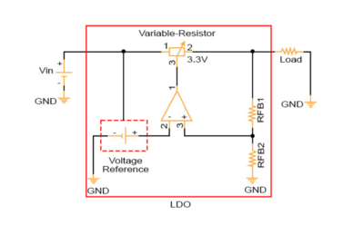
An LDO (Low Dropout Regulator) is a type of linear voltage regulator that can maintain a stable output voltage even when the difference between input and output voltage is very small.
LDO regulators provide a steady and regulated voltage for electronic circuits, remaining stable under variations in line voltage, load conditions, and even temperature changes over time.
LDOs are widely used in modern electronic systems due to the following key characteristics:
LDOs can operate with a very small voltage difference between input and output, typically from a few hundred millivolts to a few volts, making them ideal for low-voltage applications.
With strong power supply rejection ratio (PSRR), LDOs effectively suppress input noise and ripple, ensuring a clean and stable output.
Unlike switching regulators (DC-DC converters), LDOs do not rely on high-frequency switching, resulting in significantly lower output noise—ideal for analog and RF circuits.
LDOs can quickly respond to load changes, minimizing voltage fluctuations and maintaining system stability.
From smartphones and wearable devices to communication systems and embedded applications, LDOs play a fundamental role in delivering stable power.
In power PCB layout design, component placement is critical to overall performance. A poor layout can introduce noise and instability that cannot be fully corrected during routing.
The core principle is: minimize the power loop area to reduce parasitic inductance and noise coupling.
Based on the power flow (Input → LDO → Output), it is recommended to adopt a straight-line or L-shaped layout. These placement strategies help:
Avoid irregular or indirect placement that creates unnecessary current loops and noise paths.
(straight-line layout)
(L-shaped layout)
In power PCB layout, capacitor placement is critical for stability. Input capacitor should be placed close to VIN and GND. Output capacitor should be placed close to VOUT and GND. A combination of bulk capacitor + small decoupling capacitor is recommended. Proper capacitor placement helps suppress noise and ripple, optimizing both high-frequency and low-frequency response, thereby improving overall system stability.
If placement defines the structure, routing determines the actual electrical performance. In power PCB layout, the routing of power and ground directly affects voltage drop, noise, and stability.
Power traces (VIN/VOUT) and vias must be designed based on actual current requirements:
Instead of simply focusing on via order, the key is to ensure that current flows through the capacitors effectively:
This ensures proper decoupling and filtering performance.
A solid ground design is essential in power PCB layout:
Input ground and output ground should remain well connected:
Poor grounding can introduce noise coupling and degrade output voltage stability.
In summary, a well-designed LDO power PCB relies on short current loops, proper current capacity, solid grounding, and effective decoupling. With proper layout and routing practices, LDOs can deliver stable and low-noise power while avoiding common design pitfalls.
If you need support with your LDO power PCB design, the PCBWay design team is ready to help—from layout optimization to production-ready design delivery.


