The USB interface has evolved through multiple generations and now reaches the era of USB 3.1 with 10 Gbps high-speed data transfer and up to 100 W power delivery. Among them, the Type-C connector has become mainstream due to its reversible design and high compatibility. However, its high-speed characteristics also bring new challenges for PCB design. This article draws on the experience of the PCBWay design team to detail the key considerations for USB PCB design.
USB Type-C PCB Design Overview
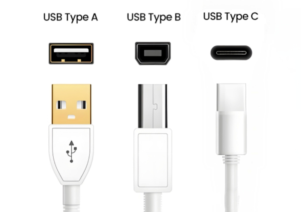
Type-C vs. Traditional USB: Key Differences and Design Challenges
- Connector and Layout: The USB Type-C connector is fully reversible and smaller than Type-A. PCB layout must be symmetrical, with high routing density, while ensuring component assembly and soldering feasibility.
- Electrical Capabilities: Type-C supports USB Power Delivery (USB PD), allowing higher current and voltage levels. Voltages can range from 5V, 9V, 15V, etc., requiring wide traces and dedicated PD controllers.
- Signal and Functionality: Type-C can handle multiple functions through the same cable. The CC pins negotiate roles and signal switching, enabling USB, DisplayPort, Ethernet, and other channels.
- Design Complexity: Designers must manage high-speed signals, intelligent protocols, high-current power, and EMI/ESD considerations. Often, multi-layer PCBs and precise simulation are required.
USB Type-C Connector and Key Pins
Connector Pin Groups
The USB Type-C connector has 24 pins arranged symmetrically. Pins are grouped as follows:
- Power and Ground: VBUS supplies 5–20V, GND is the reference. Wide copper and thermal management are required for high-current applications.
- Low-Speed / Sideband Channels: Critical pins handle connection detection, insertion orientation, power negotiation (USB PD), and role determination.
- High-Speed Data (USB 2.0): Standard USB 2.0 differential pairs ensure basic connectivity even if high-speed channels are not active.
- SuperSpeed Data (USB 3.x/4): Used for high-speed data transfer (5–10 Gbps), internal pins must strictly control impedance and differential pair lengths.
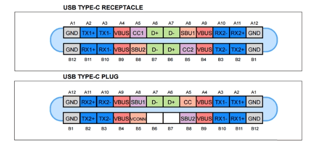
CC Pins and Reversible Insertion Detection
The Type-C specification uses CC pins with pull-up and pull-down resistors to determine device role:
- Source devices use pull-up resistors (Rp), Sink devices use pull-down resistors (Rd, typically 5.1kΩ), and Dual-Role Power (DRP) devices alternate between pull-up and pull-down.
- When a USB device is inserted, the voltage on the CC pin identifies the insertion direction (normal or reversed).
- For USB PD, CC pins also participate in power negotiation, detecting the maximum allowed current.
Understanding CC pin functionality is essential for correct PCB layout, reliable data transmission, and safe power delivery.

USB PCB Layout Guidelines
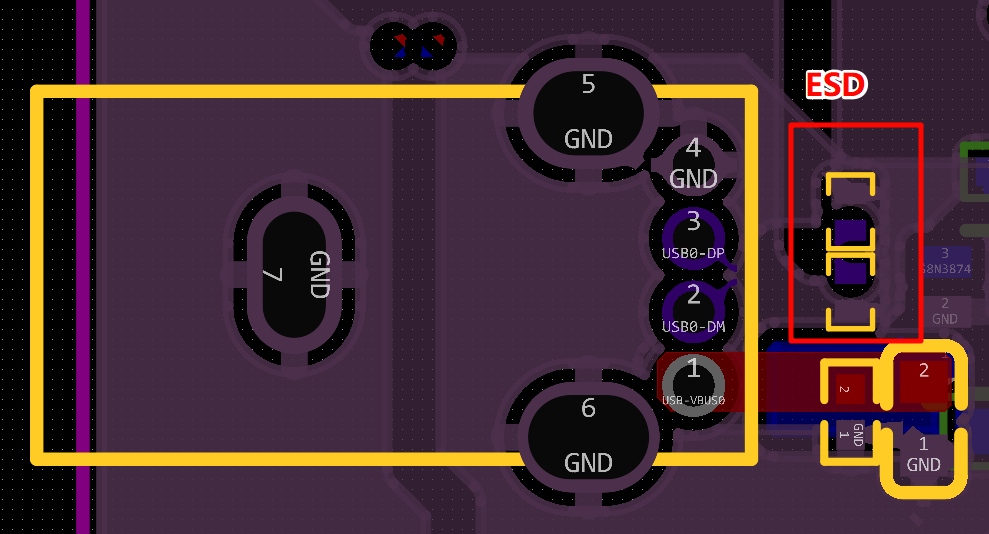
Connector Placement and Mechanical Considerations
- Position USB connectors near the PCB edge (3–5mm) to facilitate plug-in/out operations.
- Place ESD and common-mode choke devices close to the connector (≤1.5mm), in the order: ESD → common-mode choke → resistor/capacitor.
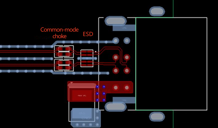
- Maintain sufficient spacing between ESD components and USB connector for post-soldering operations.
High-Speed Signal Reference Plane Design
- Ensure a continuous ground plane beneath all high-speed signals to reduce EMI.
- Avoid splits or gaps in the plane to prevent impedance discontinuities and noise coupling.
Grounding and Return Path Control
- If protective grounds (PGND) are used near USB connectors, maintain ~2mm distance from system GND and connect via ferrite beads.
- Add multiple ground vias in the protection area to ensure low-impedance return paths and suppress static interference.
Decoupling Capacitor and Local Power Placement
- Place TX signal coupling capacitors near the connector, RX signal capacitors near the device.
USB PCB Differential Pair Routing Guidelines
USB 2.0 vs. USB 3.0 PCB Routing Requirements
- Impedance: USB 2.0 differential pairs: 90Ω ± 10%; USB 3.x: strictly controlled at 90Ω.
- Grounding: Place ground copper on both sides of differential traces, with spacing ≤ 3× trace width to absorb high-frequency noise.
You can read the article comparing the design differences between USB 2.0 vs 3.0 vs 4.0 to learn more details.

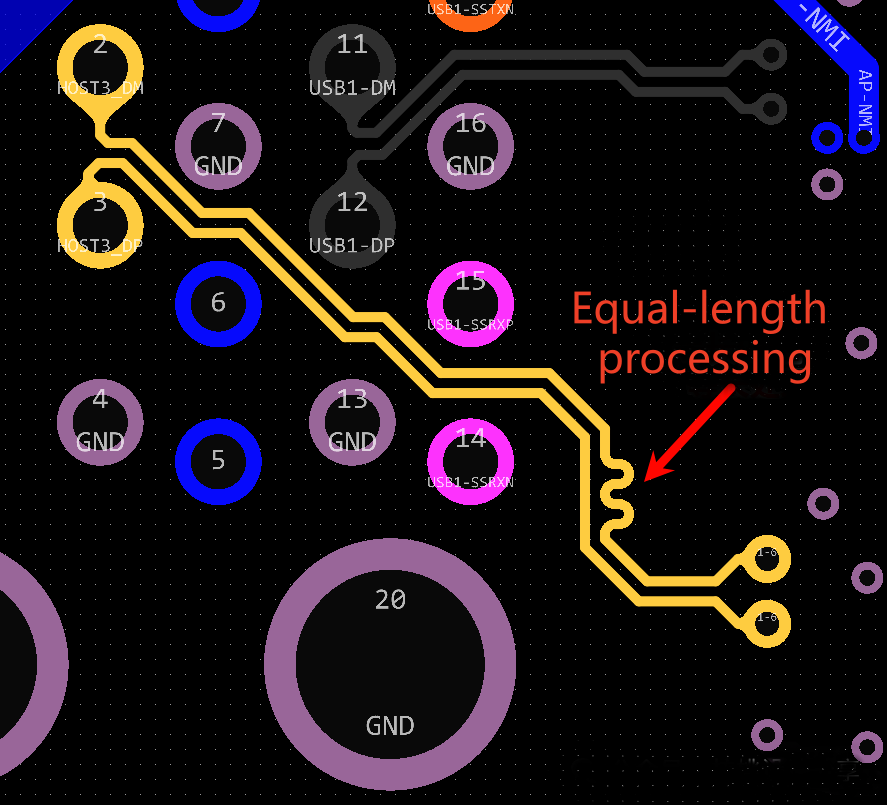
Differential Pair Length Matching and Impedance Control
- Keep trace lengths as short as possible, giving priority to routing USB differential pairs.
- Since USB signals are differential, excessive length mismatch can directly affect timing and degrade signal quality. Within a USB pair, length mismatch should be controlled to around ±5 mil. Maintain a spacing of at least 4× the trace width between adjacent pairs to minimize crosstalk.
Via Usage and Layer Transitions
- Minimize layer changes: Vias introduce parasitic capacitance; limit layer transitions to ≤2.
- Add return ground vias: For each transition, place paired ground vias adjacent to differential vias to maintain low-impedance return paths and reduce signal integrity issues.
Conclusion
When designing a USB Type-C PCB, it is essential to carefully consider connector placement, high-speed signal routing, differential pair length matching, impedance control, and high-current power paths. Following these guidelines will help ensure signal integrity, reliable power delivery, and overall device performance.
For teams seeking professional support, PCBWay’s design services offer end-to-end solutions—from layout and routing to signal simulation and production-ready design—helping you avoid design pitfalls and efficiently bring your USB Type-C PCB to mass production.
Feel free to contact us if you have any question!


