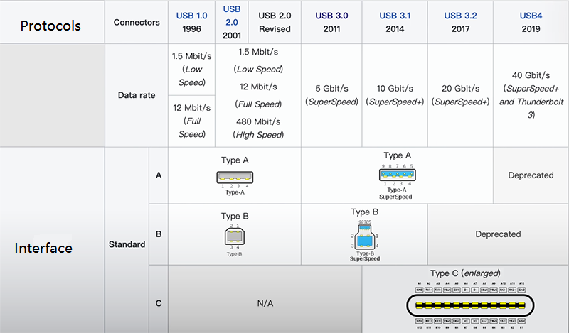
Since the USB Implementers Forum released the USB 1.0 standard in 1996, USB technology has evolved through multiple generations, including USB 1.1, USB 2.0, USB 3.0, USB 3.1, and USB 3.2. In 2019, the organization introduced the USB4 standard, bringing a new level of performance and design complexity to USB interfaces.
Different USB standards impose significantly different requirements on PCB design. In this article, the PCBWay design team provides a detailed explanation to help engineers better understand these differences, which are critical for ensuring signal integrity and overall product reliability.
Key Parameter Comparison: USB 2.0 vs USB 3.0 vs USB4
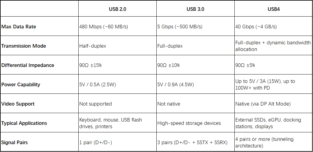
(Comparison Table)
Key Differences in USB PCB Layout
Impedance Control
- USB 2.0: Relatively loose requirement (90Ω ±15%), easy to achieve in most standard PCB stackups. The PCB manufacturer typically ensures impedance control.
- USB 3.0: Requires tighter tolerance (90Ω ±10%). Accurate stackup calculation and tighter control of trace width and spacing are necessary in USB PCB design.
- USB4: Requires ±5% or even stricter control. At very high data rates, any impedance discontinuity can directly degrade the eye diagram. Connector selection, pad design (anti-pad optimization), and overall channel design all affect impedance continuity.
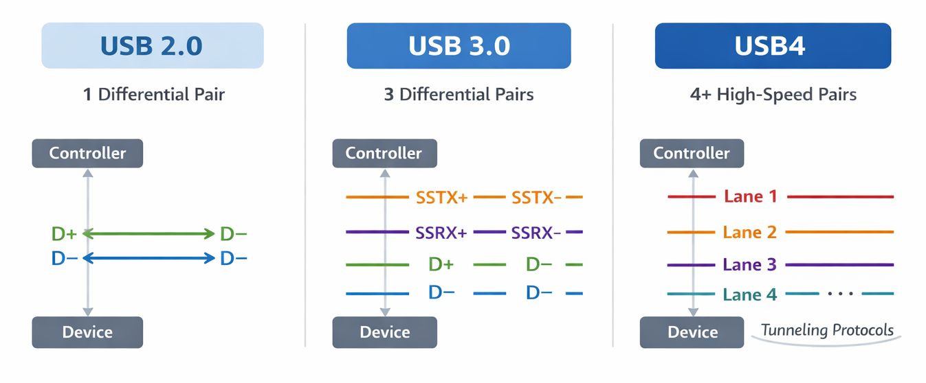
Differential Pair Length Matching
- USB 2.0: Loose requirement. The slower edge rate (~1 ns) allows tolerance of tens of mils without significant impact.
- USB 3.0: Tight intra-pair matching is required (<5 mil). TX and RX pairs are independent, and inter-pair matching is generally less critical due to protocol-level equalization.
- USB4: Extremely strict matching (<1–2 mil). Both intra-pair and inter-pair matching become important, or sufficient margin must be reserved for equalization tuning to minimize inter-symbol interference.
Routing Rules
- USB 2.0: Can tolerate 1–2 vias. At 480 Mbps, via parasitics and stub effects are relatively insignificant
- USB 3.0: Minimize vias (≤2). At 5 Gbps, via stubs introduce impedance discontinuities and reflections. Blind vias or optimized transitions are often used.
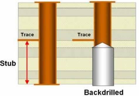
- USB4: Stub effects must be eliminated. At 40 Gbps, even a stub longer than 10 mil can cause significant reflections. Back-drilling or HDI laser vias are required in advanced USB PCB layout.
Stackup Design
- USB 2.0: 2-layer boards are possible (with coplanar waveguide), but 4-layer designs are preferred.
- USB 3.0: Minimum 4-layer stackup with a solid reference plane is required for stable impedance control.
- USB4: Typically requires 6–8 layers, stripline routing, low-loss materials, and multiple ground planes to reduce radiation and insertion loss.
EMI / SI Design
- USB 2.0: Generally not critical if basic layout rules are followed.
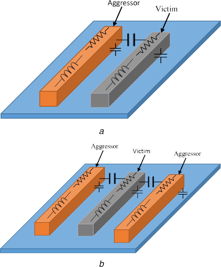
- USB 3.0: Requires attention to differential spacing, continuous reference planes, and minimizing vias and stubs.
- USB4: Becomes a core challenge in USB PCB design. Requires strict impedance control, back-drilling, optimized stackup (preferably stripline), and full signal integrity simulation (eye diagram, TDR analysis).
(Image from the internet)
Practical Design Challenges
The main challenge lies in EMI control under low-cost constraints. In 2-layer designs, coplanar waveguide structures and dense ground stitching vias are required to suppress radiation. Harmonics at 480 Mbps may still cause EMI failures if routing is not well controlled.
The key challenge is precision and crosstalk control. Impedance must be tightly controlled (90Ω ±10%), via stubs must be minimized, and crosstalk between USB 3.0 high-speed pairs and USB 2.0 signals within the same connector must be carefully managed.
The challenge is RF-level design precision across the entire signal path. At 40 Gbps, back-drilling is mandatory, AC coupling capacitor pads must be optimized, low-loss materials are required, and return paths must remain fully continuous. Any discontinuity or excessive loss can directly result in eye diagram closure, making full-channel simulation essential.
Conclusion
This article focuses on the key differences in USB PCB layout and USB PCB design across USB 2.0, USB 3.0, and USB4. As data rates increase, PCB design requirements evolve from basic routing practices to highly precise, simulation-driven high-speed design methodologies.
For more detailed USB PCB layout guidelines and best practices, you can refer to our previous article to further improve your design quality and reliability.
PCBWay design team offers comprehensive end-to-end design services, covering everything from PCB layout and routing to signal integrity simulation and fully production-ready deliverables. This helps you minimize design risks and accelerate your USB PCB design from concept to mass production with confidence.


