RF PCB design is significantly more challenging than conventional PCB design due to the effects of high-frequency signal propagation, impedance discontinuities, and electromagnetic interference. Even small layout mistakes can negatively impact wireless performance.
Through PCBWay's PCB Design Service, our engineers help customers optimize RF PCB layout, impedance-controlled routing, stackup design, and antenna integration to improve performance and manufacturability. This article summarizes essential RF PCB design guidelines for both beginners and experienced engineers.
RF PCB Design Fundamentals
Unlike low-frequency circuits, RF circuits are heavily influenced by electromagnetic wave behavior and distributed parameters. Understanding these fundamentals is essential for successful RF PCB design.
Three Key Characteristics of RF Signals
- Electromagnetic Wave Propagation
RF signals in the MHz and GHz range behave as electromagnetic waves rather than simple electrical currents. Trace length, routing angle, spacing, and surrounding structures can directly affect signal quality.
At high frequencies, current flows primarily on the conductor surface. As a result, copper roughness and surface finish significantly impact transmission loss.
PCB traces, pads, and vias introduce parasitic inductance and capacitance, which may cause impedance discontinuities, signal delay, resonance, and unwanted coupling.
Impedance Matching Principles
Impedance matching is one of the most important aspects of RF PCB design.
- The industry-standard impedance for most RF circuits is 50Ω.
- Certain antenna and video transmission systems use 75Ω.
- Impedance mismatches can cause signal reflections, increased VSWR, degraded return loss, and reduced power transfer efficiency.
- The entire RF signal path should maintain consistent impedance without abrupt changes in trace width or dielectric structure.
Standard RF PCB Design Flow
A typical RF circuit board design process includes:
- Define operating frequency, power level, impedance requirements, insertion loss targets, isolation requirements, and thermal constraints.
- Select suitable RF components with minimal parasitic effects.
- Design RF schematics including matching networks, filters, amplifiers, and power decoupling circuits.
- Plan PCB stackup and functional partitioning.
- Perform impedance-controlled routing and RF PCB layout optimization.
- Validate the design through simulation, prototyping, and measurement.
RF PCB Material Selection Guidelines
PCB material selection plays a critical role in RF performance. The most important parameters are dielectric constant (Dk) stability and dielectric loss factor (Df).
For Bluetooth, Zigbee, LoRa, and some WiFi applications, standard FR4 materials can still provide acceptable performance at a low cost. However, as operating frequencies increase, dielectric loss and Dk variation become more significant. High-performance RF applications typically require specialized laminates such as Rogers, Taconic, or PTFE-based materials.
Recommended Materials by Frequency Range
- Low-Frequency RF Applications (0–1 GHz)
Material: Standard FR4
Applications: 433 MHz wireless devices; 868/915 MHz IoT modules; Low-power RF receivers
Advantages: Low cost; Mature manufacturing process
Limitations: Higher dielectric loss at higher frequencies
- Mid- to High-Frequency Applications (1–10 GHz)
Materials: Rogers RO3000, Rogers RO4000, Taconic
Applications: Bluetooth, WiFi; 2.4 GHz ISM products; 5G Sub-6 GHz systems
Advantages: Stable dielectric properties; Lower insertion loss; Excellent production consistency
- Millimeter-Wave Applications (Above 10 GHz)
Materials: PTFE-based laminates
Applications: Automotive radar; Millimeter-wave communication systems; High-frequency test equipment
Advantages: Extremely low dielectric loss
Limitations: Higher material and manufacturing costs
Copper Foil Selection
For high-frequency RF PCB design, low-profile copper foil is recommended because it reduces conductor loss caused by the skin effect and improves signal integrity.
RF PCB Stackup Design Guidelines
PCB stackup significantly affects shielding effectiveness, return current paths, and overall EMC performance.
Standard 4-Layer RF PCB Stackup
- Top Layer: RF signals, RF ICs, filters, antennas, and matching networks
- Layer 2: Continuous solid ground plane
- Layer 3: Power distribution plane
- Bottom Layer: Low-speed digital signals and auxiliary circuitry
Stackup Design Rules
- RF signal layers should always be adjacent to a continuous ground plane.
- Avoid splitting the ground plane beneath RF traces.
- Place power and ground planes close together to improve power integrity and high-frequency decoupling.
RF Transmission Lines and Routing Rules
RF traces should be treated as controlled-impedance transmission lines rather than ordinary conductors.
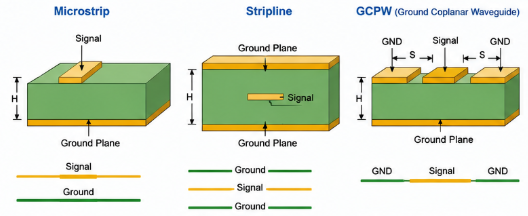
Common RF Transmission Line Structures
- Microstrip: A surface-layer trace referenced to a ground plane beneath it. Microstrip structures are simple to design and tune, making them ideal for antenna feed lines, RF input/output ports, and general RF routing.
- Stripline: A signal trace embedded between two ground planes. This structure provides excellent shielding, minimizes electromagnetic radiation, and offers superior noise immunity, making it suitable for long-distance high-frequency signal routing within the PCB.
- Grounded Coplanar Waveguide (GCPW): – A transmission line with ground copper placed on both sides of the signal trace. GCPW offers excellent isolation, improved impedance control, and reduced radiation loss, making it a popular choice for RF IC connections, antenna feed networks, and high-density RF PCB layouts.
RF PCB Routing Guidelines
- Keep RF traces as short as possible.
- Use 45° bends or curved traces instead of 90° corners.
- Avoid parallel routing between RF and digital signals.
- Follow the 3W spacing rule whenever possible.
- Minimize vias on critical RF signal paths.
- Keep test points away from primary RF transmission lines.
RF PCB Layout and Isolation Techniques
Functional Partitioning
- Separate RF, digital, analog, and power sections.
- Isolation distance should be determined based on frequency, power level, EMC requirements, and board size.
- Keep transmit and receive circuits physically separated.
- Locate oscillators, VCOs, and filters away from switching power supplies and high-speed digital devices.
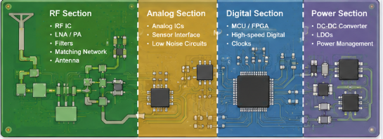
RF Signal Chain Placement
Arrange components according to signal flow: Antenna → Filter → LNA → Mixer → Power Amplifier. Linear or L-shaped placement is preferred. Avoid folded or U-shaped layouts that may introduce unwanted coupling.
Shielding Design
- Use metal shielding cans for sensitive RF sections.
- Add grounded copper guard traces around critical RF routing.
- Use via fences around RF areas to suppress EMI leakage.
RF Grounding and Power Supply Design
Grounding Guidelines
- Maintain a continuous ground plane beneath RF traces.
- Separate RF, analog, and digital ground regions and connect them appropriately.
- Add multiple ground vias around RF components, connectors, and shields.
- Use stitching vias along long ground paths to reduce ground impedance.
Power Decoupling
- Use a combination of bulk capacitors and 0.1 μF capacitors.
- Place decoupling capacitors as close as possible to power pins.
- Isolate RF power routing from noisy digital power rails.
- Utilize thermal vias and ground copper for both grounding and heat dissipation.
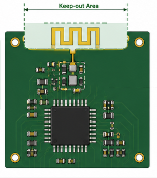
RF Antenna Layout Guidelines
In wireless products, antenna performance directly affects communication range and signal quality.
Antenna Placement
- Place antennas near the PCB edge whenever possible.
- Keep antennas away from switching regulators, batteries, displays, and digital circuits.
- Minimize metal obstructions near the antenna.
- Follow the antenna vendor's reference design recommendations.
Antenna Keep-Out Area
Most PCB antennas require a dedicated keep-out region. Requirements include:
- No copper underneath the antenna.
- No signal routing within the keep-out zone.
- Avoid mounting holes, connectors, and shielding structures in the antenna area.
Matching Network Design
A π-type matching network is commonly reserved between the RF transceiver and antenna. Benefits include:
- Antenna tuning
- Compensation for enclosure effects
- S11 optimization
- Improved radiation efficiency
Even when simulations indicate good matching, it is recommended to reserve matching network footprints for production tuning.
RF PCB Manufacturing Considerations
Many RF designs perform well in prototypes but experience issues during mass production due to manufacturing variations.
Key considerations include:
- Surface Finish: ENIG or immersion silver is preferred for RF boards due to their flat surface and stable impedance characteristics.
- Via Technology: Back-drilling or blind vias can reduce via stub effects.
- Solder Mask: Critical RF traces may be left exposed when required for tighter impedance control.
- Tolerance Control: Confirm trace width, dielectric thickness, and registration tolerances with the PCB manufacturer.
- Impedance Control: Verify target impedance, stackup parameters, and impedance tolerances. Impedance test coupons are recommended for production validation. PCBWay's impedance calculator tool can help optimize impedance-controlled designs.
Common RF PCB Design Mistakes
Mistake 1: Changing RF Trace Width Arbitrarily
Problem:
- Impedance discontinuity
- Increased signal reflection
Solution:
- Maintain a consistent controlled-impedance trace width throughout the RF path.
Mistake 2: Splitting the Ground Plane
Problem:
- Broken return current paths
- Increased noise and EMI
Solution:
- Maintain continuous ground planes beneath RF signals.
Mistake 3: Poor Ground Isolation
Problem:
- Digital noise coupling into RF circuits
Solution:
- Proper ground partitioning and controlled grounding strategy.
Mistake 4: Excessive Vias in RF Paths
Problem:
- Increased insertion loss
- Impedance discontinuities
Solution:
- Minimize vias in critical RF transmission lines.
Mistake 5: Poor Transmit/Receive Isolation
Problem:
- Self-interference and oscillation
Solution:
- Physically separate high-power transmit and low-noise receive circuits.
Conclusion
RF PCB design is a multidisciplinary process that combines electromagnetic theory, controlled-impedance routing, grounding techniques, and manufacturing considerations. Careful attention to materials, stackup design, RF PCB layout, and antenna integration can significantly improve product performance and production yield.
For complex RF projects, PCBWay's PCB Design Service provides support from schematic design and RF PCB layout optimization to impedance control and DFM review, helping customers accelerate development and achieve successful mass production.


