RF PCB layout is a critical step that determines the actual performance of a circuit, directly affecting impedance matching, signal integrity, EMC performance, and long-term stability. In the previous article, we introduced the fundamental rules of RF layout and routing. In this article, based on extensive engineering review and practical experience, we summarize 10 common mistakes to avoid in RF PCB layout. The goal is to provide practical and actionable guidance for RF design, helping engineers avoid common pitfalls and improve overall circuit reliability.
In RF PCB layout, if the trace width is not accurately calculated and the characteristic impedance is not controlled to the standard 50Ω, impedance mismatch occurs. This leads to signal reflections, degraded return loss, and inefficient energy transfer to the load, reducing actual radiated or received power.
Correct Approach:
Sudden changes in RF trace width, sharp bends, or excessive vias create discontinuities in characteristic impedance. These discontinuities degrade transmission line matching, cause signal reflections, and worsen S11.
Correct Approach:
To facilitate routing, some designers route RF signals back and forth across layers with multiple vias. Each via introduces parasitic inductance and capacitance depending on via diameter, PCB thickness, and stack-up. A typical via can introduce ~1 nH of inductance and sub-pF capacitance, which at GHz frequencies may disrupt impedance continuity, increase reflections, and even cause resonance issues.
Correct Approach:
In RF PCB layout, vias are not just interconnections,they are discontinuities that must be carefully controlled.
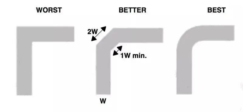
Straight 90° or sharp bends in RF traces, especially without compensation, cause local electric field concentration and effective trace width changes. This leads to impedance discontinuities, increased signal reflections, and enhanced radiation, particularly at GHz frequencies.
Correct Approach:
Floating or partially connected copper areas on the PCB can create parasitic capacitance, disturb impedance, and introduce unintended coupling between circuits.
Correct Approach:
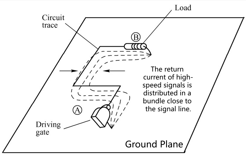
(High-speed return signals flow along the path of lowest impedance)
Placing RF traces or components close to switching power supplies or high-speed digital circuits can couple switching noise or digital harmonics into the RF path. Out-of-band noise in the receive path can reduce sensitivity, while in the transmit path it may cause spectral emissions beyond limits.
Correct Approach:
Routing traces or placing copper near the antenna can disturb the radiation field, change the effective electrical length, shift resonance frequency, reduce radiation efficiency, or cause energy loss due to metal absorption/reflection.
Correct Approach:
Placing matching components (capacitors, inductors) far from the device pins or in the middle of long traces introduces parasitic elements, ruining the designed impedance match and complicating tuning.
Correct Approach:
In RF PCB layout, the physical placement of matching networks is as important as their electrical design.
Placing decoupling capacitors far from power pins, or stacking multiple capacitors without considering effective frequency ranges, reduces high-frequency decoupling effectiveness.
Correct Approach:
Using standard FR4 at frequencies above 5GHz leads to significant dielectric and conductor loss, causing signal attenuation.
Correct Approach:
The above 10 RF PCB layout mistakes are all derived from real-world engineering reviews. They represent fundamental aspects of RF design that are commonly encountered yet often overlooked.Improving RF performance largely depends on attention to detail. Many issues encountered during the debugging stage—such as impedance mismatch, poor sensitivity, or oscillation—can often be traced back not to schematic errors, but to insufficient attention to layout details.
If you need design assistance, you can contact the PCBWay design team.


