 Mila
Jun 12,2026
143
Mila
Jun 12,2026
143
RF PCB Design Guide: Layout, Stackup, Routing and Manufacturing Best Practices
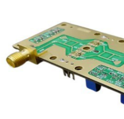
RF PCB design is significantly more challenging than conventional PCB design due to the effects of high-frequency signal propagation, impedance discontinuities, and electromagnetic interference. Even ...
Mila
Mar 17,2026
1429
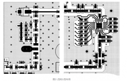
Top 10 RF PCB Layout Mistakes and How to Avoid Them
RF PCB layout is a critical step that determines the actual performance of a circuit, directly affecting impedance matching, signal integrity, EMC performance, and long-term stability. In the previous...
Mila
Dec 30,2025
3293
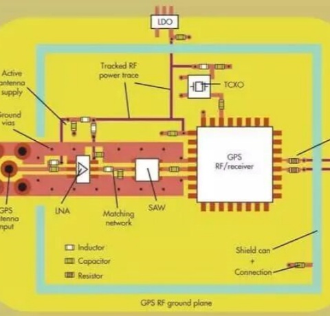
RF PCB Design Guidelines: Key Considerations for High-Frequency Circuits
In recent years, the rapid growth of Bluetooth devices, wireless local area networks (WLAN), and mobile communication systems has driven increasing attention to RF circuit design techniques. From past...
| Ranking | Name | Answers |
|---|---|---|
| 1 | Avaq Semiconductor | 1 |


