 Mila
Jun 12,2026
4144
RF PCB Design Guide: Layout, Stackup, Routing and Manufacturing Best Practices
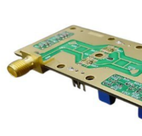
RF PCB design is significantly more challenging than conventional PCB design due to the effects of high-frequency signal propagation, impedance discontinuities, and electromagnetic interference. Even ...
| Ranking | Name | Answers |
|---|---|---|
| 1 | PCBWay Team | 7 |
| 2 | SAAD ZAFAR | 2 |
| 3 | Morad Andaloussi | 1 |
| 4 | Daniel Nebert | 1 |


