In recent years, the rapid growth of Bluetooth devices, wireless local area networks (WLAN), and mobile communication systems has driven increasing attention to RF circuit design techniques. From past to present, RF PCB design—much like electromagnetic interference (EMI) control—has remained one of the most challenging aspects for hardware engineers.
In RF PCB design, Key RF design considerations include impedance and impedance matching, dielectric materials and PCB stack-up, wavelength effects, and harmonics. This section focuses on RF PCB layout and routing guidelines, highlighting the critical factors engineers should consider when designing high-frequency circuits.
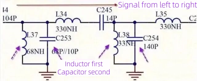
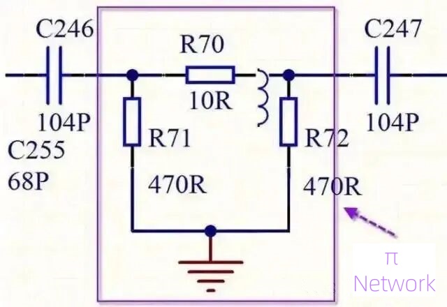
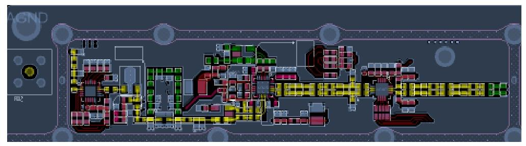
In RF PCB layout, RF signal paths should be placed first, followed by other circuits. RF chain placement should follow the schematic signal order from input to output. The sequence of components and the spacing between them are critical. Some components should not be placed too far apart, such as π matching networks.
Within the same shielding cavity, the main RF signal should be arranged in a straight line along the signal flow direction. When space is limited, an L-shaped layout may be used to avoid signal self-interference. U-shaped layouts should be avoided. If unavoidable, the distance between RF input and output should be maximized, typically at least 1.5 cm.
Antenna matching networks (such as π networks), baluns, and RF transceiver matching components should be placed as close as possible to the antenna connector, SMA port, or RF pins of the chip. This minimizes parasitic inductance and capacitance introduced by interconnects and improves impedance matching accuracy.
In RF signal routing, trace length should be minimized to reduce coupling and interference. Related RF components should be placed close together. For example, clock traces should be kept short by placing oscillators close to the devices they drive. When driving multiple devices, the routing topology should be selected based on the specific design requirements.
Right-angle or sharp bends in RF traces introduce additional parasitic capacitance and inductance. To reduce these effects, curved traces are preferred. If curved routing is not possible due to space limitations, right-angle corners should be chamfered into two 45° bends. The length of the curved or chamfered section should be at least three times the trace width.
Vias are one of the major causes of impedance discontinuity in RF signal paths. When the signal frequency exceeds 1 GHz, via effects become more significant and may lead to reflections, increased insertion loss, and phase shift.
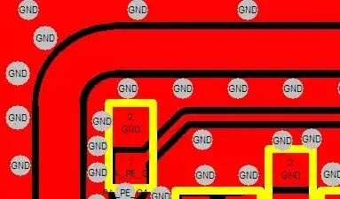
Ground traces adjacent to RF traces should be connected to the bottom or inner ground plane through vias, providing the shortest return path for interference or radiation. However, the distance between the RF signal via and ground via should not be too small, as this may significantly affect RF signal quality.
Unused portions of through-hole vias can resonate at specific frequencies (typically at λ/4 of the stub length), causing severe reflections and insertion loss notches. Blind vias, buried vias, or back drilling should be used when necessary to eliminate via stubs.
In the GHz range, via parasitic inductance and capacitance cannot be ignored. These parameters vary with via structure and stack-up and should be evaluated during the design stage using simulation or empirical rules.
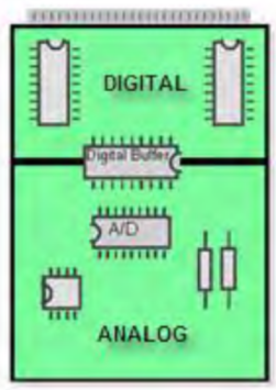
RF circuits should be clearly separated from digital and power circuits. High-noise sources such as MCUs, high-speed interfaces, and DC-DC converters should be kept away from RF signal paths and RF components to avoid interference through spatial coupling or shared return paths.
High-speed clocks, differential interfaces, and switching power signals generate strong electromagnetic radiation and should not be routed parallel to or in close proximity to RF traces. Even without direct electrical connection, coupling through electric or magnetic fields can degrade RF signal quality.
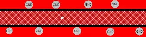
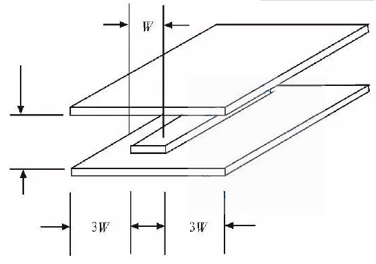
RF traces should maintain sufficient spacing from adjacent ground plane edges, typically at least 3W, with no non-ground vias within this region. RF traces on the same layer should be surrounded by grounded copper, with stitching vias added to the ground copper. The spacing between stitching vias should be less than 1/20 of the wavelength (λ) corresponding to the signal frequency and arranged uniformly. The edge of the grounded copper should be kept 2W away from the RF trace or 3H, where H represents the total thickness of the adjacent dielectric layer.
In RF circuit design, multiple disciplines such as electromagnetic theory, circuit theory, and material science must be considered, along with accumulated practical experience.
Layout and routing are critical steps in RF design. Only with well-planned layout and routing can a high-performance RF circuit be achieved, and this requires careful upfront planning and close attention to detail.
If you want a perfect RF PCB, you can choose PCBWay design service to get it!


