Overview of Differential Pair Routing
A differential pair consists of two coupled transmission lines. Differential signaling works by driving the pair with two complementary signals—one line carries the main signal while the other carries its inverse. The voltage difference between the two lines carries the transmitted information.
Basic Principles of Differential Pair Routing
1. Differential Pair Symmetry
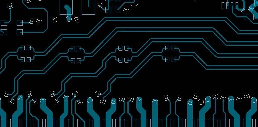
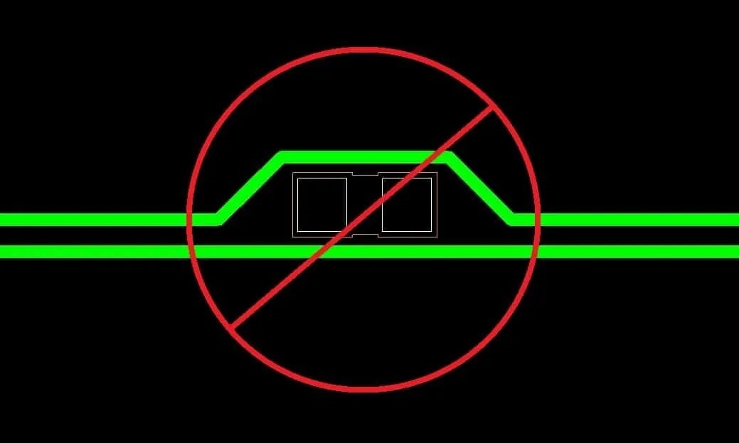
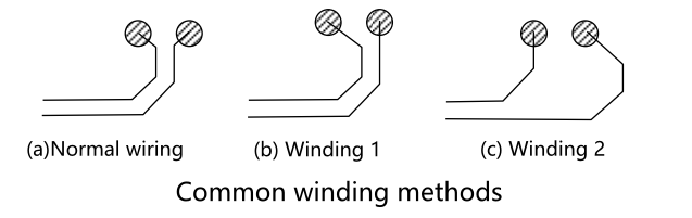
Successful differential pair routing requires the two traces to form a mirror image, both geometrically and electrically. Any asymmetry can degrade the differential structure and reduce system performance. During routing, plan paths to avoid obstacles such as vias or passive components, maintaining symmetry.
2. Differential Pair Length Matching
Length matching ensures that the signals on each line propagate with the same delay, keeping the two differential signals in opposite polarity at all times. Any delay mismatch converts part of the differential signal into common-mode, degrading signal quality.
- Intra-pair length differences should be kept very small, typically within 5–10 mils.
- Shorter traces can be extended using serpentine routing to match lengths.
- Manual tuning is often required near IC pins due to layout and pin placement constraints, minimizing impedance discontinuities.
3. Differential Pair Spacing
Maintaining consistent spacing within the pair ensures continuous differential impedance and reduces reflections.
- Intra-pair spacing should be uniform, typically with a trace-to-trace ratio of 1:1 to 3:1.
- Spacing that is too small increases manufacturing difficulty; spacing that is too large reduces differential coupling.
Differential Impedance Control
Definition and Target Values
Differential impedance is the characteristic impedance of two tightly coupled traces, calculated approximately as:
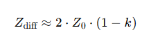
where kkk is the coupling coefficient (0 < k < 1). Tighter coupling (smaller spacing) increases kkk and decreases Zdiff.
Typical target values:
- 100 Ω: Widely used (Ethernet 10/100/1000/10G Base-T, HDMI, DisplayPort, SATA, SAS, MIPI, etc.)
- 85 Ω: PCI Express series (PCIe 1.0 to PCIe 6.0)
- 90 Ω: USB 2.0/3.x/4, Thunderbolt
- 120 Ω: Industrial buses (RS-485, CAN) and DDR4/5 DQS differential pairs
Impact of Trace Width, Spacing, and Dielectric Thickness
- Increasing trace width → lowers impedance (largest effect)
- Increasing spacing → raises impedance (weaker coupling)
- Increasing dielectric thickness → raises impedance (electric field more spread out)
Problems from Impedance Discontinuities
- Signal reflection: causes overshoot, undershoot, and ringing; may degrade eye diagrams and increase BER.
- Common-mode noise generation: reduces receiver CMRR and increases EMI.
- Timing jitter: introduces deterministic jitter, reducing timing margin.
Differential Pair Reference Plane and Layer Selection
Relationship with Continuous Reference Planes
Differential pair impedance and signal integrity depend on an adjacent reference plane. Route differential pairs over continuous reference planes whenever possible to maintain stable impedance and reduce EMI.
Avoid Crossing Split Planes
Crossing split or interrupted reference planes breaks return paths, causing reflections and common-mode noise. In multilayer designs, reroute or add stitching vias to maintain continuity.
Preferred Layers in Multilayer Boards
- Prefer inner layers close to a continuous reference plane, avoiding outer layers exposed to air.
- For high-speed interfaces, signals are typically routed on layers adjacent to a GND plane.
Return Path Considerations
Differential return currents flow along the reference plane. Discontinuities increase crosstalk and reflections. Maintaining plane continuity, minimizing cross-plane transitions, and proper via placement ensure good signal integrity.
Differential Pair Vias and Layer Transitions
Crossing a PCB layer via a via introduces parasitic elements, so via count should be minimized.
- Symmetry: Both vias of a differential pair must be symmetric in position, size, and electrical characteristics to maintain P/N signal integrity and avoid timing skew. Critical for high-speed interfaces (PCIe, USB3.x, HDMI).
- Spacing: Intra-pair via spacing should be consistent, typically ≥3× trace width for impedance continuity. Inter-pair spacing should follow the 3W rule to reduce crosstalk and common-mode noise.
- Via Type Selection: Choose through-hole, blind, or buried vias according to design requirements.
- Blind/Buried vias: Reduce via length and parasitic effects but increase fabrication complexity and cost.
- Through vias: Simple and cost-effective, but may leave long stubs, requiring back-drilling optimization.
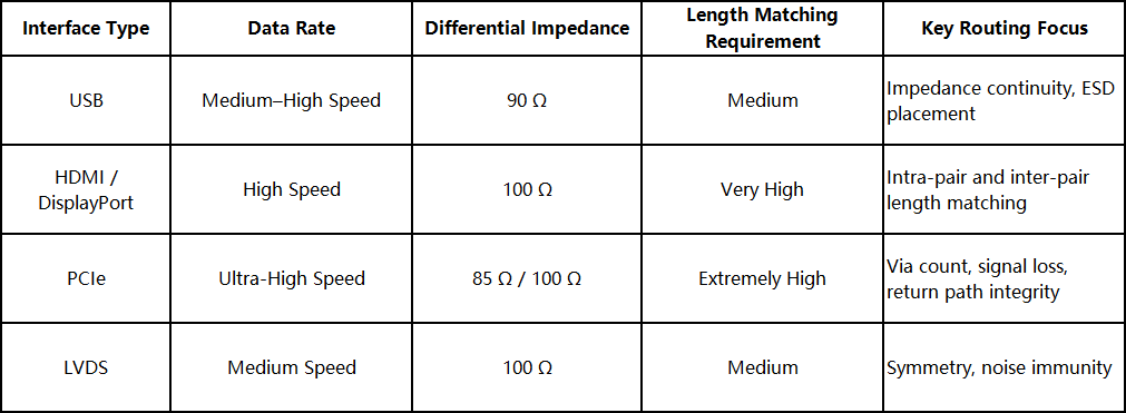
Differential Pair Routing Considerations for Different High-Speed Interfaces
Differential Impedance:
- PCIe: 85 Ω ±10% (per generation specification)
- USB: 90 Ω ±10%
- HDMI: 100 Ω ±10%
Intra-Pair Length Tolerance:
- PCIe (Gen4+): ≤5 mil
- USB: ≤5 mil
- HDMI: Strict intra-pair and inter-pair matching, depending on HDMI version
Via Count:
- PCIe: Minimize via count; P/N vias must be symmetric
- USB 2.0: ≤2 vias recommended; USB 3.x: minimize vias
- HDMI: Minimize vias; symmetric vias with ground stitching vias recommended
Conlusion
Differential pair routing is the lifeline of high-speed digital design. Through precise symmetry and strict length matching, it fundamentally determines signal integrity, timing accuracy, and noise immunity, forming the physical foundation for stable, high-speed system operation. The key to success lies in establishing and rigorously following a set of quantifiable, simulation-verified routing rules, proactively addressing potential issues from the earliest design stages.
If you need design assistance, you can contact the PCBWay design team. We will provide you with the best design services.


