In PCB design, layout is a critical stage that directly determines the quality of the routing. A well-organized layout ensures efficient signal paths and reliable power distribution — the first and most important step toward successful PCB design.
Simply put, PCB layout design is the process of arranging all components based on their functional structure and modular relationships, while meeting DXF and mechanical constraints to ensure smooth placement and routing.
Component placement and routing together define the signal integrity and power integrity of a circuit board. A successful PCB layout is built upon four key principles: shortening the signal path, controlling impedance, ensuring proper return paths, and constructing a low-impedance power network — all working together to preserve clean signals and stable power delivery.
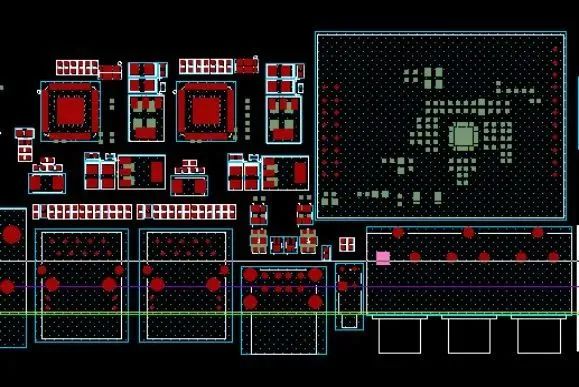
Before placement begins, divide the schematic into clear modules such as the power supply section, digital core, analog circuits, RF module, and I/O interfaces, and assign each a distinct physical area on the PCB.
Grouping related components within the same area not only simplifies debugging and testing but also helps isolate noise between functional blocks, effectively preventing mutual interference.
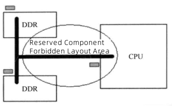
High-frequency and low-frequency circuits behave differently, and EMC design must be a key consideration. High-speed devices (e.g., CPUs and DDR memory) should be placed close together to minimize critical trace lengths. Meanwhile, sensitive low-frequency analog circuits (e.g., sensor amplifiers or precision reference sources) should be positioned far from high-frequency digital regions. Physical separation between digital and analog domains is essential to reduce coupling and noise.
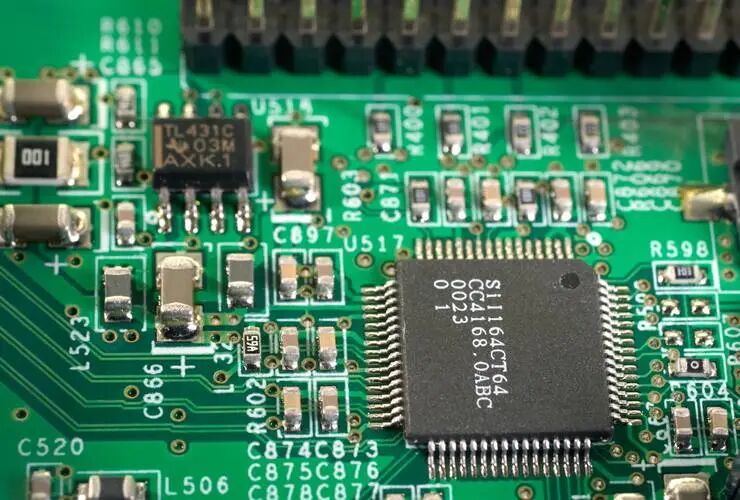
For switching power supplies, the power loop (input capacitor–chip–inductor–output capacitor) must be laid out compactly to suppress switching noise. Decoupling capacitors should follow the “as close as possible” rule — with high-frequency capacitors placed directly next to IC power pins and connected to ground vias with the smallest possible loop area.
Additionally, maintain solid power and ground planes to provide complete return paths for high-speed signals and prevent resonance, ensuring both signal purity and power stability.
Thermal Design: Place heat-generating components such as CPUs or power ICs near ventilation openings or chassis edges for better heat dissipation. You can read this article for more on thermal management in PCB layout.
Mechanical Constraints: Begin by placing immovable components like connectors (power, USB, Ethernet), switches, LEDs, and mounting holes. Ensure adequate clearance between components, board edges, and mounting holes to avoid mechanical interference during assembly.
1.Control Characteristic Impedance: Precisely calculate and maintain the characteristic impedance of transmission lines to eliminate reflections and waveform distortion.
2.Length Matching for Critical Signals: Apply strict length matching to key signals such as clocks and data buses to prevent timing skew.
3.Maintain Continuous Reference Planes: Keep an unbroken ground reference under signal traces to provide the shortest return path — essential for impedance control and signal integrity.
4.Use Proper Termination: Apply series or parallel termination resistors at line ends to absorb reflected energy and maintain clean, stable signals.
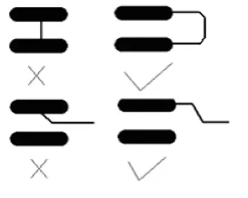
1.Ensure Impedance Continuity: Avoid impedance discontinuities caused by vias or sharp corners; design smooth, consistent transitions for high-speed and differential pairs.
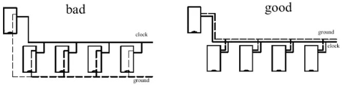
2.Provide a Short and Complete Return Path: Never route high-speed traces over split planes. When layer transitions are necessary, place ground vias nearby to minimize loop inductance and EMI.
3.Equal Length and Equal Spacing for Differential Pairs: Differential traces must maintain identical lengths and constant spacing throughout their route to prevent conversion of differential signals into common-mode noise.
4.Symmetrical and Tight Coupling: Differential pairs should be routed symmetrically on the same layer and closely coupled to ensure external noise is evenly coupled and effectively canceled.
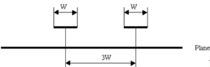
Minimize Crosstalk through Spacing and Shielding: Follow the 3W rule and reduce parallel runs between high-speed or sensitive traces to suppress crosstalk.
1.Use Planes Instead of Traces: Continuous planes provide low-impedance paths, effective decoupling, and clear reference surfaces for high-speed signals — essential for both power and signal integrity.
2.Widen High-current Paths: Calculate the required width based on current density and allowable temperature rise (following IPC standards), then increase width to reduce IR drops and heating.
3.Connect Decoupling Capacitors Directly to IC Pins: Place capacitors as close as possible to the IC’s power pins, using short, wide traces for minimal parasitic inductance.
4.Isolate Different Voltage Domains: Clearly separate power rails with different voltages to prevent coupling and short-circuit risks.
5.Use Multiple Vias for Power and Ground Connections: Multiple vias reduce connection impedance and prevent local current bottlenecks and hotspots.
6.Avoid Ground Loops: Always maintain a continuous ground plane; if splitting is unavoidable, use single-point grounding to prevent loop antenna effects and reduce noise emissions.
For more details, you can read this article.
An optimized PCB placement enables high-quality routing, maximizing usable space and potentially reducing the number of layers, thereby lowering manufacturing costs. The layout phase establishes the foundation for both power and signal integrity — errors made here are nearly impossible to fix later during routing.
Routing constraints have a direct influence on layout decisions. Parameters such as trace width, spacing, impedance, timing, via count, and EMC rules all determine component placement and board area allocation. For example, high-speed or differential pairs require equal-length routing and clear paths, while power traces must remain short and wide. Therefore, routing channels and zoning must be reserved during the layout phase. Ignoring these constraints often leads to routing difficulties and degraded signal or power integrity. In short, layout must be designed for routability.
Predefine Physical Channels for Impedance Control: Accurately set dielectric thickness, trace width, and copper weight to achieve precise characteristic impedance for high-speed and differential signals.
Build a Low-impedance Power Distribution Network (PDN): Utilize adjacent power and ground planes to form planar capacitance for efficient decoupling and noise suppression.
Ensure Short and Complete Return Paths: Each signal layer should have an adjacent reference plane, connected with stitching vias to maintain minimal loop area for high-frequency return currents.
A well-executed PCB layout design establishes a strong foundation for signal and power integrity through functional zoning, critical path optimization, and precise decoupling capacitor placement. It also determines overall routing complexity and manufacturing cost.
Routing, on the other hand, translates design intent into reality — its quality directly determines the success of the entire board. Effective routing relies on controlled impedance, complete return paths, and accurate length matching to transform electrical connections into high-quality signal channels.
Only when layout and routing work in close collaboration can a design achieve the optimal balance between functionality, performance, and manufacturability. Together, they define the electrical performance, reliability, and cost efficiency of any PCB design.
Feel free to ask us if you have any question.


