In intelligent switched-mode power supply design, the current-loop layout of an AC-DC converter is critical to the overall system performance. A well-designed layout can improve power efficiency, reduce electromagnetic interference (EMI), and ensure system stability and reliability.
In power PCB design, current loops are among the most critical aspects to be addressed. The primary objective is to minimize the area of key current loops as much as possible, thereby reducing voltage spikes and radiated interference caused by parasitic inductance.
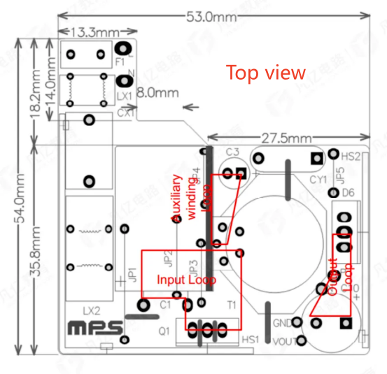
In a typical flyback AC-DC power supply, the following three current loops require particular attention and optimization.
1. Primary Switching Loop
The primary switching loop is one of the highest di/dt and strongest EMI sources in an AC-DC power supply. Its typical current path is: C_bulk → transformer primary winding → switching device Q1 → current sensing / return path → C_bulk.
This loop should be made as compact as possible. The bulk input capacitor (C_bulk) must be placed close to the switching device and the transformer primary to minimize loop area, thereby reducing switching spikes, voltage ringing, and radiated EMI.
2. Auxiliary Winding Loop
The auxiliary winding loop is typically used to supply power to the control circuitry. Its current path is: T1 (auxiliary winding) → D4 → R4 → C3 → T1.
Proper layout of the auxiliary winding loop can effectively reduce voltage spikes caused by leakage inductance, thereby lowering transformer-related electromagnetic interference and switching losses. In addition, a well-designed auxiliary winding improves the transformer’s autotransformer ratio and energy conversion efficiency, enhancing overall electrical performance.
3. Secondary Rectification Loop
The output rectification loop is a low-voltage, high-current loop with the following path: T1 (secondary winding) → D6 → C10 → T1.
This loop should use short, wide, and direct copper traces and be placed as close as possible to the rectifier diode and output capacitor. Doing so minimizes conduction losses and reduces EMI radiation on the secondary side.
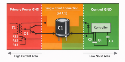
1. Ground Separation: Single-Point Connection Between Power GND and Control GND
In AC-DC power supplies, the input power ground carries large currents and high di/dt noise, whereas the control ground serves as a low-level, small-signal reference. If these grounds are extensively mixed, switching noise can easily couple into the control and feedback circuitry through ground paths, leading to jitter or malfunction.
Therefore, the power ground and control ground should be physically separated and connected at a single point only—typically at the negative terminal of the bulk input capacitor (C1). This ensures a clear and controlled high-current return path while providing a clean ground reference for the control circuitry.
(AC-DC GND Segmentation & Optocoupler lsolation)
2. Layout of Switching Device Q1 Heatsink and Main Ground
The switching device Q1 is the dominant source of high dv/dt and di/dt noise in an AC-DC converter. Its heatsink often has parasitic capacitive coupling to the drain or main ground. If sensitive signal traces are placed nearby, high-frequency noise can be capacitively coupled into the control circuitry.
In PCB layout, the heatsink of Q1 can be referenced to the main power ground plane. Additionally, copper clearance or cutouts around the heatsink area are recommended to reduce noise coupling into nearby circuits. Sensitive traces such as feedback and gate-drive signals should be kept away from the heatsink region.
3. Protecting the Feedback Trace: Keep It Short and Away from Power Paths
The feedback trace is one of the most sensitive signals in a power supply, as it directly participates in closed-loop regulation and typically operates at a low signal level. Any noise coupling into the feedback path may increase output ripple, cause duty-cycle jitter, or even destabilize the control loop.
Therefore, the feedback trace should be routed away from switching nodes, the transformer primary, and rectifier diodes. Its length should be minimized, and where necessary, routing close to signal ground or using ground shielding can further improve noise immunity.
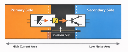
4. Optocoupler Isolation: Enhancing Primary-to-Secondary Isolation with PCB Cutouts
The optocoupler provides signal transfer between the primary and secondary sides, and its isolation performance depends not only on the component itself but also heavily on PCB layout. Insufficient copper clearance or traces crossing the isolation boundary can degrade isolation and introduce common-mode noise coupling.
To improve isolation, PCB cutouts or increased creepage distance should be implemented beneath and around the optocoupler. The copper and routing on the primary and secondary sides must be clearly separated, thereby enhancing electrical isolation and overall noise immunity of the system.
(Optocoupler lsolation)
In summary, a successful AC/DC power supply PCB design requires meticulous control over details, standards, and EMI. From “safety first” considerations such as high-voltage clearance and isolation, to the “foundation of performance” in power loops and grounding strategies, and finally to the “green passport” of EMI filtering and layout techniques, every aspect is essential. Keeping these points in mind and incorporating them into your design checklist can significantly improve the reliability, efficiency, and compliance of the power supply, eliminating potential risks from the outset and creating an “energy heart” built to withstand the test of time.
The core principle of AC-DC PCB layout is “safety and isolation,” while the core principle of DC-DC PCB layout is “noise and current loop control. If you’ve finished reviewing the key AC-DC PCB design considerations and would like to learn more about DC-DC PCB layout, you can continue with the following article:
DC-DC Converter PCB Layout Guidelines: Power Loops, Hot Loops, and EMI Control
If you need the help of the AC-DC converter PCB layout, you can contact PCBWay design team to help you!


