DDR3 layout and routing are highly demanding, requiring careful attention to signal integrity, timing, and design constraints. The following summarizes the key design process, component placement strategies, and routing considerations to ensure stable and reliable system performance.
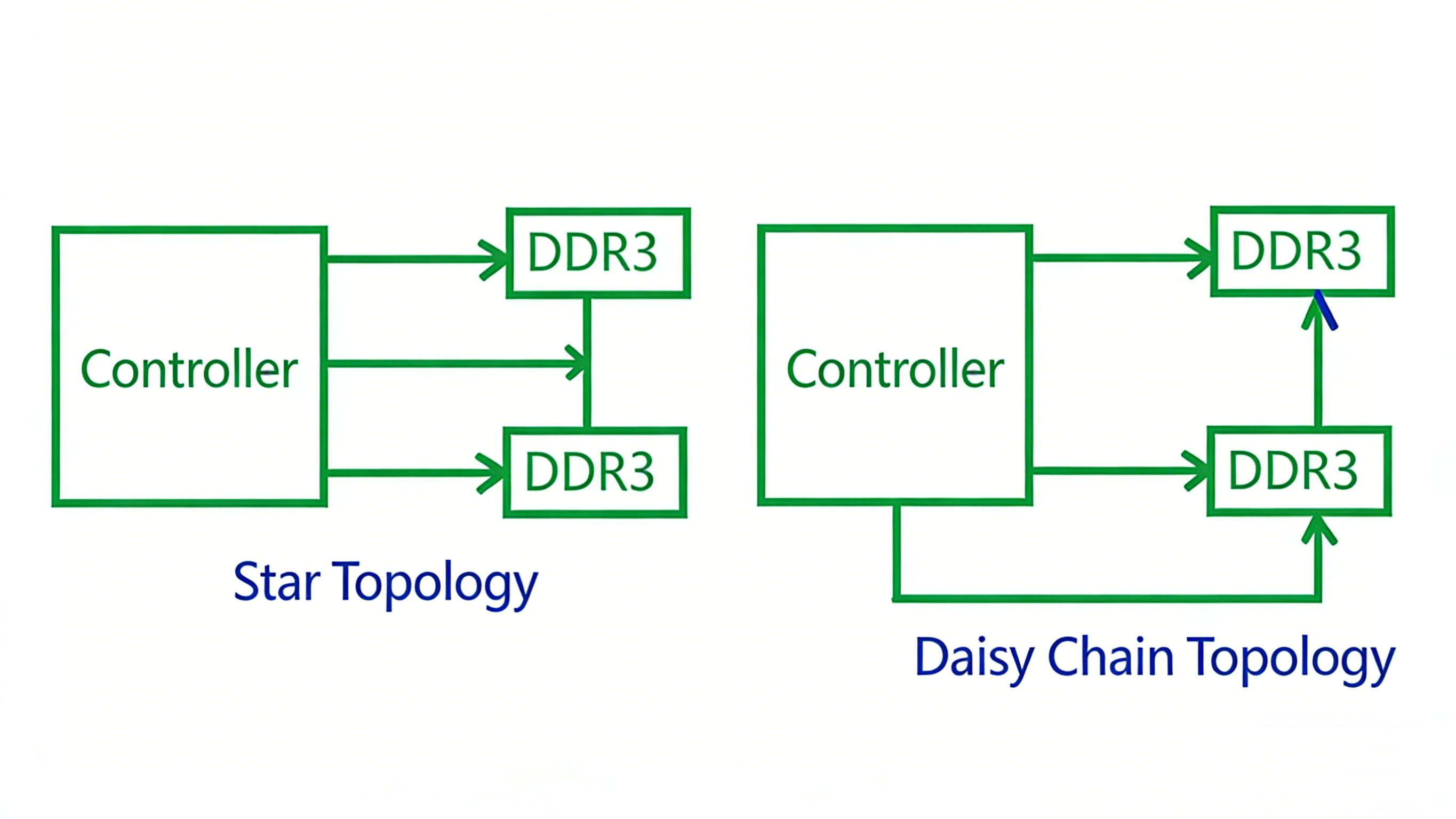
DDR3 Topology Design and Selection Guidelines
1. Data Signal Topology
Data signals include DQ, LDM, UDM, LDQS, and UDQS. All data signals use a point-to-point connection, where each DDR3 device is directly connected to the controller. Data signals do not involve a choice between T-Topology or Fly-by routing; instead, the focus is on length matching and signal integrity control.
2. Address and Control Signal Topology
Address and control signals include A0–A14, BA0–BA2, CLK, CKE, RAS, CAS, CS, WE, and RESET, among others. Topology selection depends on whether the controller and memory devices support read leveling and write leveling. When read/write leveling is supported:
- 2–4 DDR3 devices: either T-Topology or Fly-by routing may be used.
- Four or more DDR3 devices: Fly-by topology is recommended to achieve better timing margin and compatibility.
Topology selection mainly affects the routing of address, control, and clock signals and does not change the point-to-point nature of data signals. In practical DDR3 designs, Fly-by topology is commonly preferred due to its good compatibility, flexible timing adjustment, and relatively easier routing.
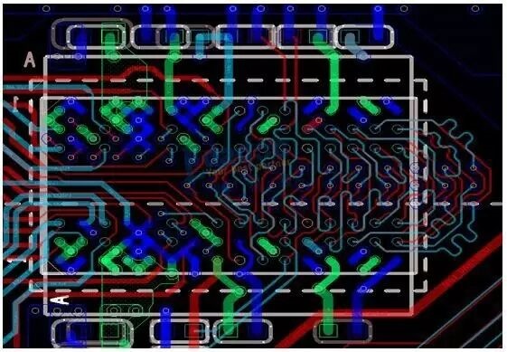
DDR3 Component Placement Guidelines
The placement of DDR3 components directly affects signal integrity and timing margin. The following principles should be observed:
- DDR3 devices should be placed as close as possible to the controller to minimize critical signal length, reduce propagation delay, and improve signal quality.
- Data-related pins should be positioned close to the corresponding controller pins, shortening the routing distance of DQ and DQS signals and facilitating length matching and timing control.
- Decoupling and bulk capacitors should be placed as close as possible to the DDR3 power pins. Power traces should be wide and short to minimize loop area and improve power stability.
(VDD capacitor placement)
- VTT termination resistors should be placed at the end of the address signal routing, typically near the last DDR3 device, or at the furthest T-point in a T-topology, to ensure proper termination.
(VTT filtering capacitor)
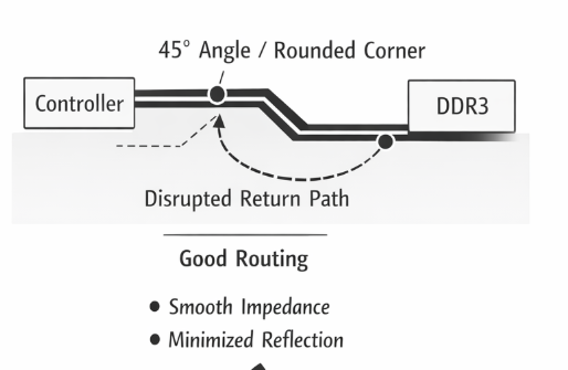
DDR3 Routing Basic Rules
In DDR3 PCB design, routing quality has a direct impact on signal integrity and system stability. The following basic rules should be followed:
- All signal traces should be kept as short as possible to reduce propagation delay and signal reflections, thereby increasing timing margin.
- Sharp angles and right-angle corners should be avoided. It is recommended to use 45° bends or smooth curves to reduce impedance discontinuities and reflection risks.
- Minimize the number of vias, as vias introduce additional parasitic inductance and impedance discontinuities that can degrade high-speed signal quality.
- Ensure all signal traces have a continuous and complete reference plane, either a ground plane or a power plane. For AC signals, ground and power planes are equivalent in terms of AC potential at high frequencies.
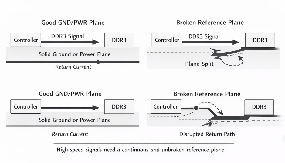
- Avoid breaking the reference plane due to vias or plane splits whenever possible. Although this is difficult to completely avoid in practice, it should be treated as an important design objective.
- After completing address and data signal routing, all DDR3 power pins, ground pins, and the power/ground connections of decoupling capacitors should be routed first, to avoid interference with subsequent length matching and to reduce routing difficulty.
Conclusion
By properly planning the topology structure, carefully arranging component placement, thoughtfully grouping signals, and following strict routing rules, the signal integrity, timing margin, and overall system stability of DDR3 PCB layouts can be significantly improved, leading to more reliable high-speed memory performance.
If you need assistance with PCB design or PCB layout, feel free to contact the PCBWay Design Team!


