As one of the core components of an inverter, the transformer directly affects the overall system efficiency and reliability. In PCB layout design, the transformer’s placement, surrounding environment, and routing paths must be carefully planned to minimize power loss, electromagnetic interference (EMI), and thermal issues.
To reduce high di/dt current loop areas, the transformer should be placed close to the main switching devices and the rectification/filtering circuits. Shorter power paths help reduce parasitic resistance and inductance, thereby improving efficiency.
Transformers generate significant heat during high-power operation. Adequate thermal design must be considered during layout. Avoid placing the transformer close to electrolytic capacitors, optocouplers, voltage references, or MCUs. Airflow direction should also be considered, especially for vertically mounted transformers, and sufficient copper area or heat dissipation structures should be provided.
The layout around the transformer should take electromagnetic compatibility into account. Proper shielding and noise control techniques should be applied to minimize radiated and conducted interference affecting both the system itself and nearby electronic devices.
A transformer is not a component that can simply be placed wherever space allows. It is a key element in power PCB design that simultaneously determines EMI performance, safety compliance, and long-term reliability.
The transformer should be oriented so that its secondary side (output side) routing is perpendicular to nearby high-frequency or high-speed signal traces, reducing mutual coupling and interference.
The transformer should be placed as close as possible to the main power switching devices to shorten high-current paths and minimize conduction and switching losses.
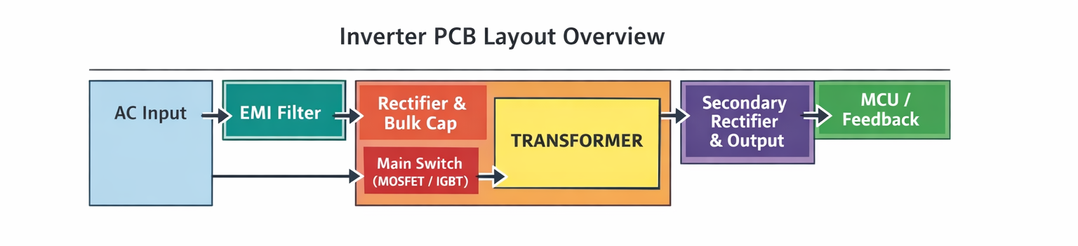
A typical layout sequence is: AC input → EMI filter → rectifier → bulk filter capacitors → transformer.
This ensures that common-mode and differential-mode noise is sufficiently suppressed before reaching the transformer.
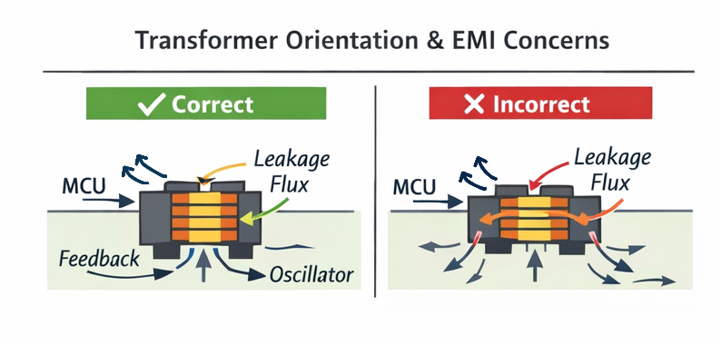
Magnetic flux leakage is inherent at the core joint. To minimize magnetic coupling that could cause signal distortion, reference drift, or system instability, a core orientation with the joint perpendicular to the PCB plane is preferred. If horizontal mounting is used, the leakage flux direction should be oriented away from control ICs, feedback loops, oscillators, and other sensitive circuits.
The secondary rectification nodes exhibit high dv/dt switching noise. Power ground and signal ground should be properly isolated, secondary high-current traces should maintain sufficient spacing from control signal lines, and long parallel routing should be avoided. When necessary, use perpendicular trace crossings to reduce coupling.
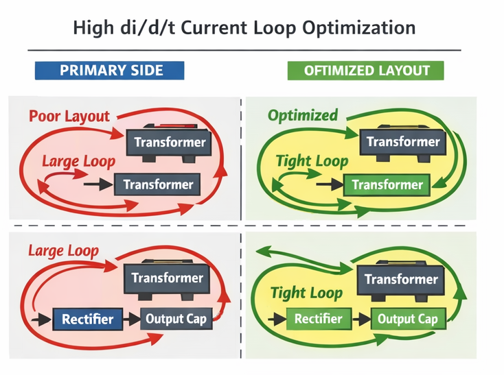
1. Primary side:MOSFET → Transformer → Current sensing → MOSFET. Use wide and short copper traces to form compact triangular or rectangular loops. Kelvin connections should be applied at the current sensing resistor terminals.
2. Secondary side: Transformer → Rectifier → Output capacitor → Transformer. Rectifier diodes should be placed close to the transformer pins, and output capacitors should be located near the rectifier outputs to minimize loop area.
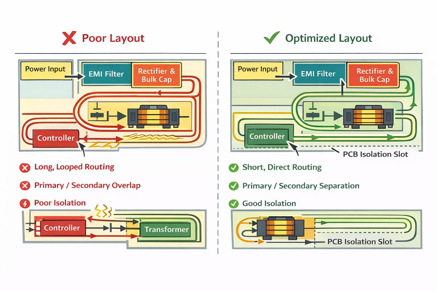
1. Avoid long parallel routing between primary and secondary traces. When crossing is unavoidable, use 90-degree crossings to reduce coupling.
2. Increase creepage distance by introducing PCB slots. Isolation slots of approximately 1.0–1.5 mm under the transformer can increase creepage distance to 2–3 times the safety requirement, reducing leakage risks caused by contamination.
1. Minimize vias in high-frequency, high-current paths. Each via introduces approximately 0.5 nH of inductance. If vias are unavoidable, use multiple small-diameter vias in parallel.
2. Avoid closed-loop routing structures that may act as loop antennas. Keep signal trace lengths below λ/20 (λ being the wavelength of the highest relevant frequency). Ferrite beads or common-mode chokes may be used when necessary.
1. Avoid unnecessary plane splits beneath the transformer. If plane splitting is required, ensure complete isolation between primary and secondary ground planes.
2. Ensure all control signals have clear and continuous return paths. A solid ground plane should be placed beneath the control IC, with analog and digital grounds connected at a single point.
Before finalizing the PCB design, electromagnetic field simulation and validation of the transformer layout are strongly recommended. Simulation helps identify potential layout issues early in the design phase and allows for targeted optimization, reducing costly redesigns and improving overall system robustness.


