In the previous LED PCB Layout article, we discussed several practical considerations for LED PCB layout and routing. Proper placement and routing are essential for achieving reliable LED performance. In this article, our design team will take a deeper look at the thermal aspects of LED PCB design, including thermal resistance, heat flow paths, and how PCB layout affects heat dissipation. Understanding these fundamentals helps designers create more efficient and reliable LED PCB layouts.
Although LEDs are often called “cold light sources,” their electro-optical conversion efficiency is not 100%. In most commercial LEDs, the efficiency is typically 20%–30%, which means that about 70% of the electrical energy is converted into heat rather than light. This unavoidable energy loss is the fundamental reason why LEDs generate heat. Even with improvements in luminous efficiency, a portion of the energy will always be dissipated as heat.
When the PN junction temperature becomes too high, it can directly affect LED performance and reliability:
For this reason, thermal management is a critical part of LED PCB design and LED PCB layout.
Definition: Thermal resistance (θ) is a physical quantity that describes a material’s resistance to heat transfer.
Physical meaning:
A lower thermal resistance (θ) indicates better heat conduction and improved heat dissipation performance.
Electrical analogy:
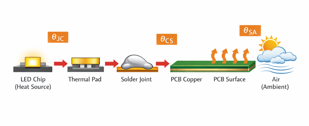
The thermal path can be understood using an electrical circuit analogy:
Series rule:
Heat must travel through multiple materials from the LED junction to the ambient air. The total thermal resistance is therefore the sum of each layer:
Understanding this concept is essential for optimizing LED PCB layout and thermal design.
In most LED PCB designs, heat flows through a multi-stage thermal conduction path:
1. Junction → Package (θJC): Heat first travels from the LED PN junction to the thermal pad or package base. This internal thermal resistance is defined by the LED manufacturer as θJC (junction-to-case thermal resistance).
2. Package → PCB Pad: Heat then transfers through the solder layer from the LED package to the PCB pad. The solder quality and contact area directly affect the thermal resistance at this interface.
3. Heat spreading inside the PCB: The PCB acts as the main path for heat spreading. In LED PCB layout, factors such as copper area, copper thickness, and thermal via distribution determine how efficiently heat can spread across the board.
4. PCB → Ambient Air (θSA): Finally, heat dissipates from the PCB surface to the surrounding air through convection and radiation. This stage is known as θSA (sink-to-ambient thermal resistance).
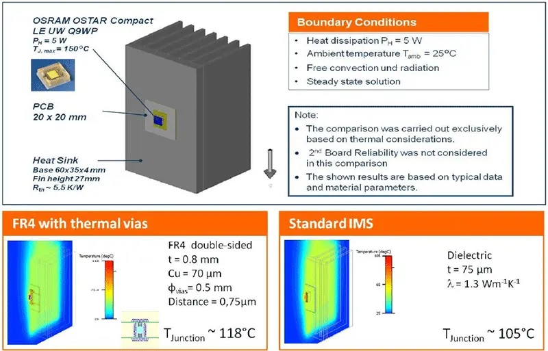
Proper LED PCB design and layout can significantly reduce thermal resistance and improve reliability.
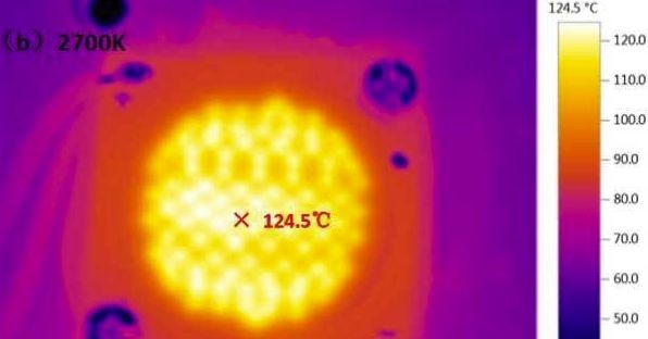
(Image from internet)
If you're looking for a custom LED PCB, you can choose PCBway's design team to assist you with the design and production.


