LED PCBs are not merely passive carriers; they are critical systems that determine the final performance, lifespan, and quality of a product. Their design directly impacts optical efficiency, reliability, and cost. Successful layout and routing must address core challenges from the outset, including uniform brightness and color temperature, efficient heat dissipation, and long-term operational stability. The PCBWay design team will share key considerations and best practices for LED PCB layout and routing based on our design experience.
In LED PCB design, the goal is to deliver stable, uniform current to each LED or string using constant-current drivers and low-impedance power distribution, ensuring consistent brightness and color. LEDs should be evenly arranged based on photometric and thermal considerations, with copper pours, thermal vias, and metal substrate paths planned to manage heat effectively. This integrated approach supports long-term reliability and product lifespan.
Proper component placement is the foundation of LED PCB design. A well-planned layout not only ensures uniform brightness and color temperature but also simplifies subsequent routing and supports thermal and mechanical reliability.
LED arrays should be placed symmetrically around the PCB’s physical or optical center. This ensures that electrical paths (line length, impedance) and thermal paths (to heat sinks or board edges) from the driver circuit to both edge and central LEDs are as symmetric as possible, minimizing current and temperature deviations caused by positional differences.
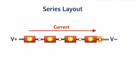
1. Series-only: LEDs should be arranged according to the electrical connection order, in a straight line or a folded path.
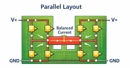
2. Parallel-only:Typically use “H-pattern” or grid-shaped power distribution, with LEDs evenly connected to the low-impedance network, preventing current imbalance caused by uneven path lengths.
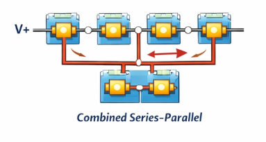
3. Mixed (series-parallel):First, ensure LEDs within each independent series branch are sequentially arranged. Then, all parallel branches should be physically symmetric and consistent across the board.
The traces from the driver IC to LEDs carry switching or constant current. Minimizing distance reduces line resistance, voltage drop, and power loss, improving system stability.
Centralized layout:
Pros: Concentrates heat sources for targeted thermal management and simplifies mechanical design.
Cons: May create local hotspots, potentially causing color shift and accelerated lumen depreciation.
Distributed layout:
Pros: Promotes more uniform heat distribution across the PCB and heatsink, reducing peak temperatures.
Cons: Raises baseline temperature of the board and may complicate integration with compact heat sinks.
The choice depends on board size, cooling strategy, and mechanical constraints.
Thermal performance is largely determined during the layout stage. Even with the same materials and copper thickness, different component placements can significantly affect heat dissipation paths and junction temperature distribution.
High-power LEDs and drivers often have bottom thermal pads. These pads should align with primary heat dissipation areas. Pads floating in air or near board edges restrict heat flow into the PCB, reducing overall thermal efficiency.
Critical thermal paths should remain continuous and unbroken. Unnecessary splits or cutouts create thermal bottlenecks, preventing uniform heat dissipation and causing local hotspots. Thermal copper areas should be pre-planned during layout to ensure smooth heat flow.
Thermal vias should be evenly distributed under or around heat sources, forming a regular array to improve vertical heat transfer. Coverage should span the entire heat source area, with slightly higher density at the center if needed.
Envision the primary thermal path from heat source to final heat sink: chip → pad → PCB copper → via array → backside copper/heat sink → environment. Layout should preserve this path, avoiding interruptions from mounting holes, slots, or cutouts.
This is the core of LED PCB electrical performance, directly affecting current stability, brightness uniformity, and system reliability.
According to electromagnetic theory, a current loop acts like an antenna, and its radiation or reception efficiency is proportional to the loop area. Current loops should be as short and direct as possible to minimize parasitic inductance, EMI, and voltage overshoot.
To further suppress parasitic inductance and magnetic radiation while maintaining signal integrity, main supply traces (VLED+ and GND) feeding the LED array should run in close, parallel pairs. Their magnetic fields cancel each other, significantly reducing loop inductance.
The path from the power source to the first LED, and from the last LED back to the current-sense resistor, must be as straight and short as possible. Any unnecessary bends increase resistance, causing voltage drop (ΔV = I × R_trace). Define clear main and branch circuits to ensure each line carries its intended current.
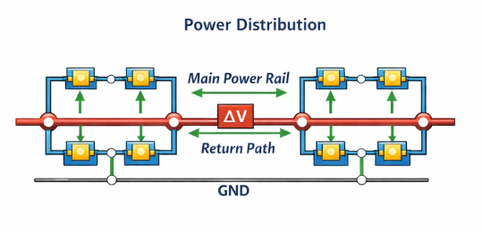
Main trunk:
Pros: Extremely low impedance, can carry high currents with minimal voltage drop, providing a stable voltage reference for all branches.
Cons: Branches closer to the power input may experience slightly higher voltage than distant branches due to trunk voltage drop.
Branch supply:
Pros: Symmetric routing ensures each parallel branch experiences the same impedance (including main trunk to branch contact resistance and branch trace resistance), achieving uniform current distribution.
Typically, a main trunk with symmetric branches is used: first, establish a low-impedance trunk, then draw symmetrical branches to each load.
For series LEDs, the current is the same through each device. The key is to ensure each LED experiences an even voltage drop. Use short, equal-width traces in sequence, managing the total chain voltage to guarantee sufficient voltage at the last LED.
In parallel LED configurations, uneven trace length or shape can cause some branches to carry higher current, resulting in brightness inconsistency or overheating. Ensure all parallel branches from the supply point to loads have identical trace length, shape, and number of vias to enforce impedance matching.
In mixed configurations, total power must be evenly distributed to ensure each series unit receives balanced supply. Use wide copper pours as “power buses,” with each series branch connected at symmetric locations from the bus in an identical manner.
LED PCB design is a precise integration of optical, thermal, and electrical performance. The key to success lies in planning the layout with thermal management as the priority, achieving current uniformity through symmetric and balanced physical placement, and ensuring electrical integrity with the shortest, low-impedance paths. Only by systematically coordinating these factors can high-quality LED products with uniform brightness, stability, and reliability be achieved.
If you're looking for a custom LED PCB, you can choose PCBway's design team to assist you with the design and production.


