During the PCB design process, component placement plays a critical role. A well-planned and scientific layout not only makes the board look clean and organized, but also effectively controls trace length and routing complexity. High-quality component placement has a significant impact on overall system performance. This article shares several practical details that can help improve PCB layout quality.
Trace width and spacing have a major impact on overall board performance. Trace width affects current-carrying capacity, temperature rise, and impedance control (especially for high-speed signals). Trace spacing influences crosstalk, EMI performance, and manufacturing yield. Trace width and spacing should be determined by comprehensively considering these factors, rather than simply increasing width or spacing without proper analysis.
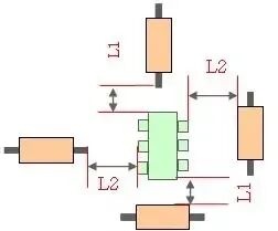
Component spacing is a critical consideration during PCB layout. Insufficient spacing can easily lead to solder bridging and manufacturing defects.
Recommended Spacing:
Proper spacing helps ensure soldering reliability and production quality.
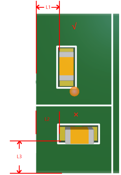
When designing PCB layout and routing, adequate clearance from the board edge must be carefully considered.
In mass production, panelization is commonly used to improve efficiency. If components are placed too close to the board edge, mechanical stress during depanelization may cause pad lifting or component damage. Similarly, traces routed too close to the edge may crack due to board deformation during separation, potentially leading to circuit failure.
Recommended Distances and Placement Guidelines:
It is recommended that component pads be placed parallel to the V-cut direction in panelized boards. This ensures that mechanical stress during depanelization is applied uniformly along the same direction, reducing the risk of pad lifting.
Distance from component body to board edge: ≥ 0.5 mm
For panelized boards with V-cut:
Component to V-cut: ≥ 0.5–1.0 mm
Pad to V-cut: ≥ 0.3 mm
Trace to board edge: ≥ 0.5 mm
In high-density or RF designs, smaller distances may be acceptable, but manufacturing tolerances must be carefully evaluated.
The size and placement of vias significantly affect circuit performance. Proper via design must consider current capacity, signal frequency, and manufacturing capability.
Key Via Design Considerations:
If you need assistance with PCB design or PCB layout, feel free to contact the PCBWay Design Team!


