During the PCB layout stage, functional zoning should always be performed before placing any components. Jumping directly into component placement often leads to higher costs during routing, debugging, and EMI control in later design stages.
Dividing the circuit into different functional zones—such as analog, digital, power, and RF—is one of the fundamental principles of PCB layout. Proper functional partitioning effectively reduces interference between different modules and minimizes noise coupling risks.
For example, in order to minimize shared return paths between analog and digital signals, analog signal processing circuits should be physically isolated from digital signal processing circuits in the layout. In addition, high-frequency RF circuits are typically placed in dedicated zones to reduce electromagnetic interference (EMI) to other parts of the system.
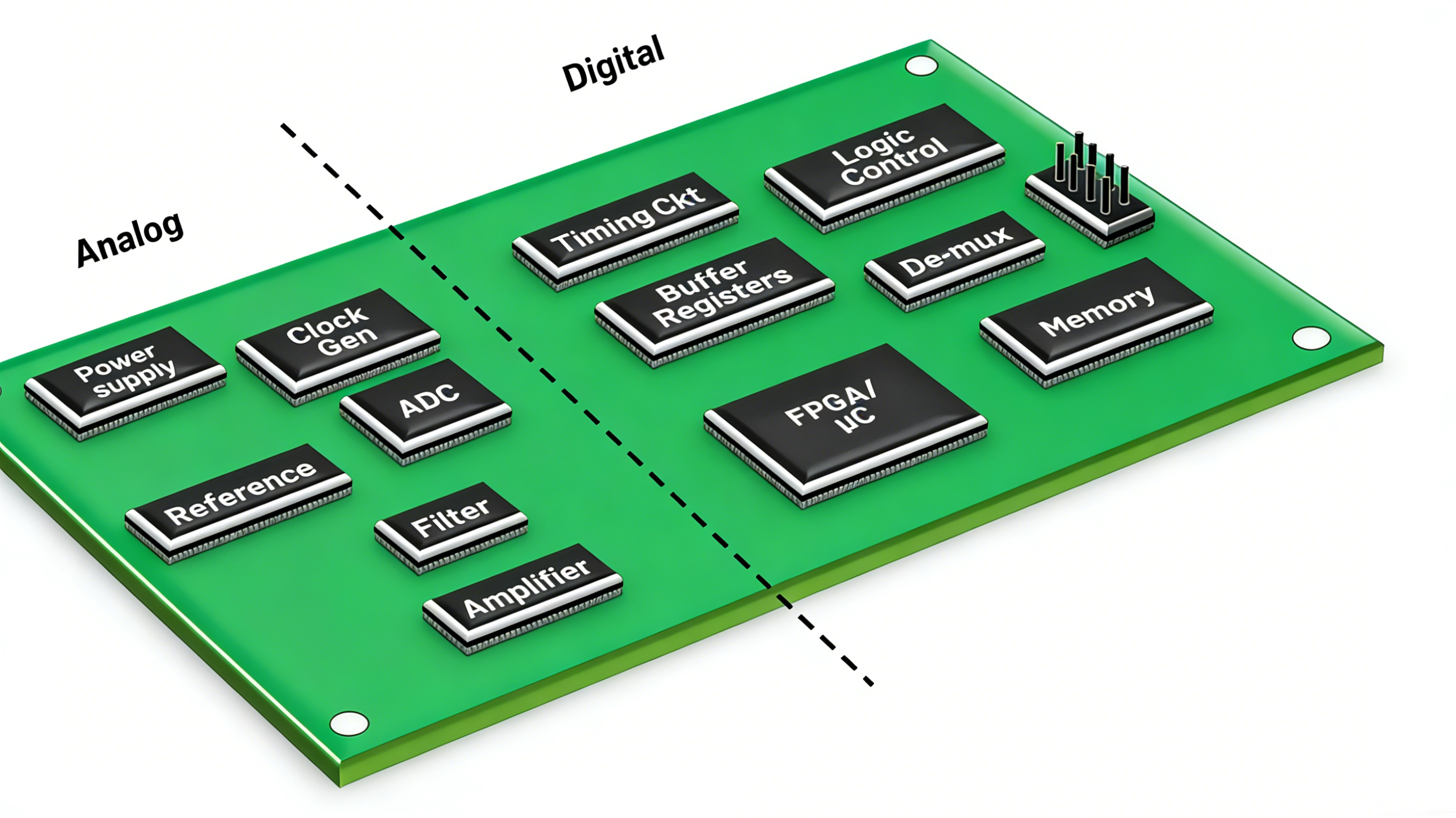
When placing high-voltage, high-current, or strongly radiating components (such as transformers and power amplifiers), they should be kept as far as possible from low-current, low-voltage, and noise-sensitive components (such as sensors and low-noise amplifiers).
By increasing the physical distance between noise sources and sensitive circuits at the layout stage, noise coupling, crosstalk, and system stability risks can be significantly reduced.
Components that are constrained by mechanical or structural requirements should be placed first. Once their positions are fixed, the placement of other components usually needs to be arranged around them. Typical mechanically constrained components include external connectors such as USB, HDMI, Ethernet, and power connectors. These components are usually placed along the PCB edges or at predefined locations to meet enclosure and assembly requirements.
Next, place special components and large functional devices in the circuit, such as heat-generating components, transformers, and ICs. These components often determine power distribution paths, signal routing directions, and thermal structure. Their placement should facilitate shorter critical traces, reduced noise, and improved thermal performance.
After the positions of core components are determined, passive components such as resistors, capacitors, and inductors can be placed. Passive components offer greater placement flexibility and are typically arranged later in the layout process to optimize routing efficiency.
Power is a critical part of any circuit and must be handled carefully. In general, power modules should be placed close to the components they supply while remaining properly isolated from other circuit sections. Power-related components should be placed compactly, with appropriate decoupling to ensure power integrity.
To reduce inductance and prevent current limitation, power traces should be short, straight, and implemented with wide copper traces.
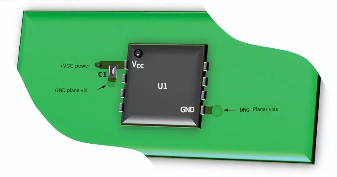
Decoupling capacitors should be placed as close as possible to the power pins of the devices they support. To minimize additional series inductance, these capacitors should be connected to a low-impedance ground plane using short traces or vias.
For each critical signal, the signal source and destination should be clearly identified, and components should be arranged according to the signal transmission direction whenever possible. Signal paths should be as short and direct as possible, avoiding unnecessary detours.
Improper component placement often forces signal traces to backtrack, detour, or cross other signals. This not only increases routing complexity but also introduces risks of crosstalk and noise coupling.
By arranging components properly at the placement stage, signal crossings and cross-zone routing can be minimized, resulting in a cleaner and more controllable layout.
Connectors are typically the entry and exit points for signals on a PCB, and their placement should maintain a reasonable relationship with the corresponding core components.
General recommendations include: placing high-speed interface connectors as close as possible to their associated processing chips; ensuring signal paths from connectors to core components are direct and do not pass through unrelated functional zones; and maintaining adequate spacing between different connectors to reduce mutual interference.
Component placement on a PCB is critical to electronic design success. Proper layout ensures manufacturability and reliability, enhances signal integrity, reduces electromagnetic interference, and improves thermal, mechanical, and test performance. From high-speed signal quality to power integrity and long-term reliability, well-planned placement bridges circuit design and physical implementation, forming the foundation for high-performance, stable electronic products.
If you need design assistance, you can contact PCBWay design service.


