As electronic devices continue to deliver more functionality while shrinking in size, advanced component packaging technologies have become essential to meet these demands. Since its introduction, BGA has remained one of the most widely adopted packaging technologies for high-performance and high-density electronic designs.
In this article, we take a closer look at BGA packaging and discuss the key PCB layout considerations for reliable BGA implementation.
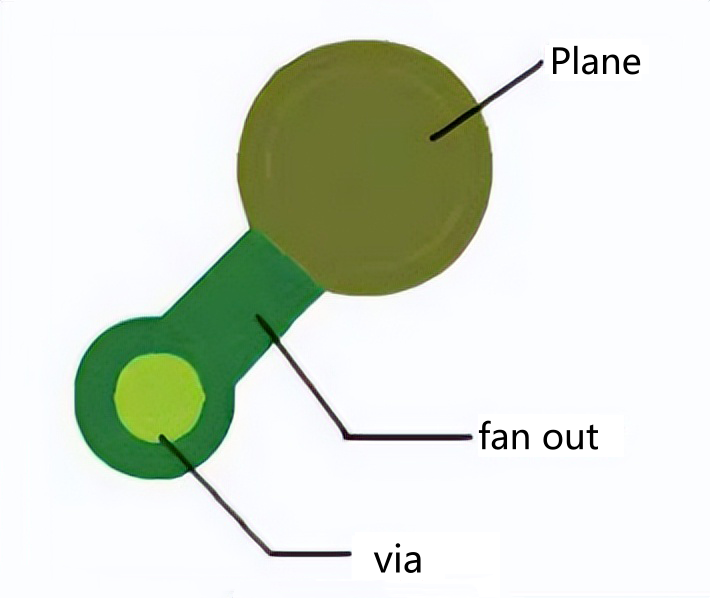
Fanout refers to the short routing from a component pad to a nearby via, as shown in the figure below. In PCB layout—especially for BGA designs—fanout, pads, and vias play a critical role.
The first task in BGA layout is to plan the routing or “fanout” strategy. Fanout is not simply drawing a short trace and placing a via; it must be planned in conjunction with component placement, layer stack-up, signal integrity requirements, and routing density.
The entire PCB layout should be organized around the BGA, particularly the main processor or SoC. The BGA is the source and destination of most signals and power connections, making it the natural center of the layout, with other components arranged around it.
Continuous reference planes are the foundation of both signal integrity and power integrity. Ground and power plane partitions must be planned early in the layout stage, and high-speed signals should never cross split reference planes.
The more complex the BGA device, the more critical early planning becomes to ensure that every ball can be successfully routed to its corresponding net.
BGA components should be placed near the center of the board or at positions that minimize critical signal path lengths. Priority should be given to the relative placement of high-speed connectors (such as Ethernet or SFP+), memory devices (DDR, Flash), and power management ICs.
High-speed memory, clock sources, and power management devices should be placed as close as possible to the BGA to minimize signal length, impedance discontinuities, crosstalk, and latency.
At the same time, BGA components should be kept away from board edges or connectors, where routing space is limited and mechanical stress can compromise reliability.
When multiple high-density BGAs are present on the same PCB (such as “CPU + FPGA” or “SoC + GPU”), sufficient spacing and routing channels must be reserved between them. Each BGA requires adequate space for complete fanout and clean routing to prevent congestion and interference.
Board edges experience the largest thermal gradients and mechanical stress during reflow soldering. BGAs placed too close to the edge may suffer from uneven heating, increasing the risk of cold joints, opens, or solder defects. It is generally recommended to maintain a clearance of at least 7–10 mm between the BGA edge and the PCB edge.
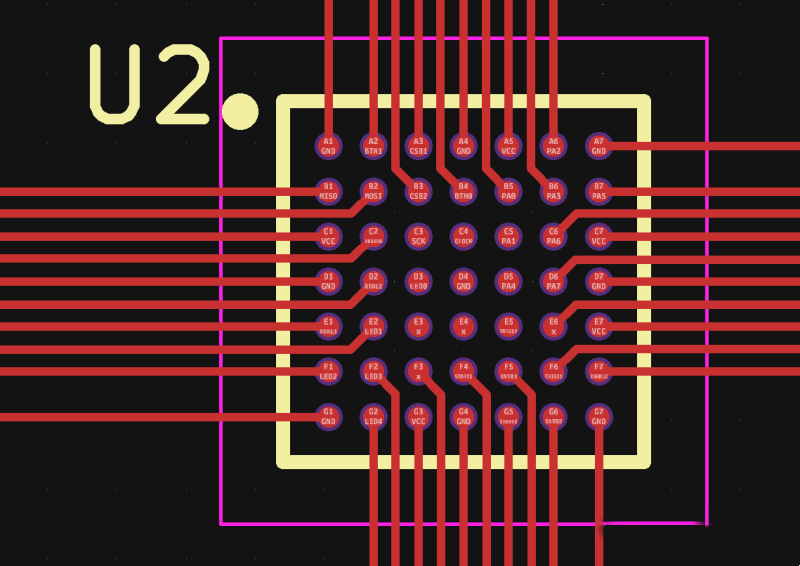
The outer rows of BGA balls—especially the first one or two rows—should receive the highest priority during fanout and routing. These balls have more available space and can typically be routed directly or with minimal bends, preserving routing channels for inner balls. If outer-row routing resources are consumed too early, inner balls may become impossible to fan out, forcing the use of blind/buried vias or additional layers.
Inner balls, especially those from the third row inward, present the greatest fanout challenge due to limited space. Common approaches include using dog-bone fanout or microvias to route signals to inner layers. Fanout should proceed from the outside inward, ring by ring, ensuring each row has a clear and repeatable breakout strategy.
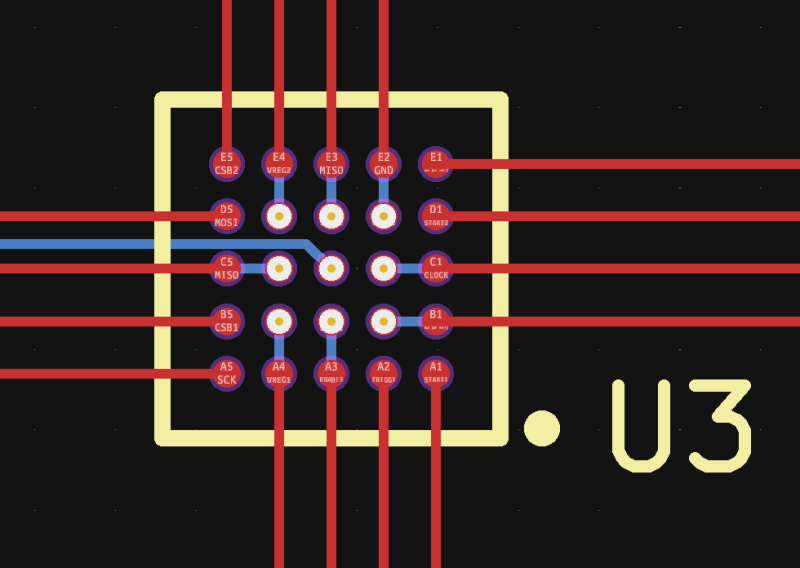
Dog-bone fanout is the classic and widely used BGA breakout style. It consists of a short trace (“neck”) extending from the pad to a via (“head”). This approach is well suited for standard through-hole vias or designs where laser microvias are limited. When routing density is high or layer count is constrained, dog-bone fanout can be arranged in different directions to improve breakout efficiency.
Via-in-pad is another BGA routing technique, typically used for ultra-fine-pitch BGAs where it is impossible to place vias between adjacent pads. In this approach, vias are placed directly in the pads and signals are routed outward on inner layers. Via-in-pad layouts should follow consistent rules across the entire BGA and avoid mixing multiple fanout styles within the same device to reduce manufacturing and assembly risks.
This is an advanced principle that reflects both manufacturability and reliability. Symmetrical and consistent fanout patterns promote uniform heat distribution, improve signal integrity, and enhance PCB manufacturability and readability.
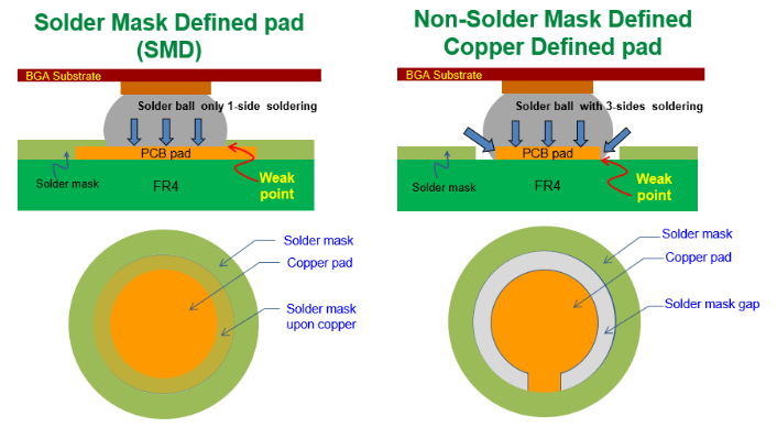
The choice between NSMD and SMD pads directly affects layout flexibility. NSMD pads offer a larger solderable area because the solder mask opening is larger than the copper pad, resulting in better solder joint formation and reduced stress concentration at BGA joints. They also provide more routing space between pads and are widely preferred for BGA designs. SMD pads, while offering stronger pad adhesion in some cases, further reduce pad spacing and increase the risk of solder mask misalignment and bridging.
The minimum distance from the via annular ring edge to any SMT pad edge should be ≥ 3–4 mil (0.075–0.1 mm). If vias are placed too close to pads, the solder mask bridge between them becomes extremely narrow and may break during fabrication, negatively impacting solder joint quality.
Via-in-pad with filled and plated vias can significantly improve fanout and routing density, particularly for small-pitch BGAs. However, this technique should be applied consistently across the BGA region to avoid unnecessary manufacturing complexity and assembly risk.
The solder mask bridge is the only physical barrier preventing solder bridging between adjacent SMT pads. Its minimum achievable width is a key factor in determining the minimum allowable component pitch. During layout, designers should fully consider solder mask capability limits and use tools such as PCBWay DRC to verify manufacturability.
Routing directions should be kept as consistent as possible. Adjacent signal layers are typically routed orthogonally—for example, horizontal routing on L1, vertical routing on L2, and horizontal routing again on L3. This approach minimizes interlayer crosstalk, simplifies routing intersections, and improves overall routing efficiency.
Each layer transition introduces an impedance discontinuity (via stub) and a change in return current path. For high-speed signals—especially those above 1 GHz—layer transitions should ideally be limited to no more than one. Preferred routing layers should be defined during the fanout stage to avoid unnecessary layer switching within the BGA area. Ideally, a signal should exit the BGA pad, pass through a single via to its target layer, and route directly to its destination.
BGA PCB layout is a highly systematic engineering task performed within extremely limited space. Its goal is not only to achieve maximum interconnection density, but also to ensure signal integrity, power stability, and solder joint reliability, ultimately resulting in a robust and reliable PCB.
If you need design assistance, you can contact the PCBWay design team. We will provide you with the best design services.


