As electronic devices continue to shrink in size, their internal circuits must also become smaller. Product miniaturization has become a strong industry trend, creating new challenges for engineers working on compact PCB designs. When designing PCBs in limited space, engineers often integrate external components into the internal structure to reduce part count. However, reducing the solution size often introduces performance trade-offs. The following sections outline the essential constraints that must be defined before starting a tight-space PCB design.
Board Size Limitations
Functional Module Definition
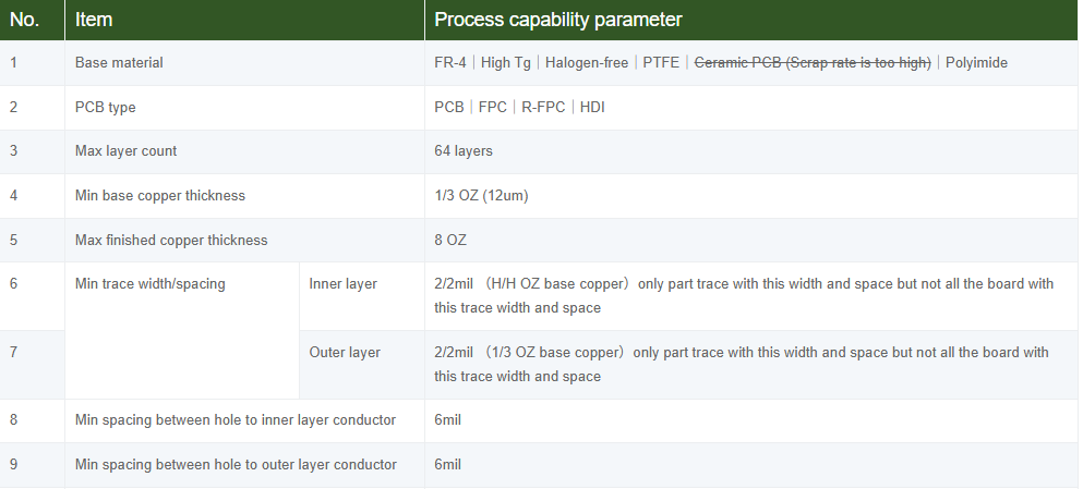
Manufacturing and Process Constraints
Key fabrication limits directly affect limited space PCB design feasibility:
Signal Types and Critical Network Requirements
Compact and tight-space PCB design requires early identification of sensitive or high-speed paths:
Functional Block–Based Placement
Treat the PCB not as scattered components but as structured modules. Grouping circuits into logical blocks simplifies routing and reduces congestion in space-constrained PCB layouts. (e.g., power module, LDO module, MCU with its decoupling network, DDR memory module, USB interface module, sensor conditioning circuitry, etc.)
Grouping Highly Related Component
In compact PCB designs, short signal paths improve stability. Examples:
Prioritize the Placement of Critical Components
The placement process should follow a clear priority. Core components determine the structural “skeleton” of the entire PCB, so their positions must be fixed early in the layout stage.
Orientation and DFM Considerations
Layout planning must consider not only electrical performance but also whether the design can be manufactured efficiently and reliably:
Avoid Congestion Hotspots
In tight-space PCB design, it is very easy for certain areas to become overly congested, leaving no room for routing. These issues must be anticipated and resolved during the early layout phase:
Vertical and Horizontal Space Utilization
Region Segmentation
Dividing areas improves noise control and routing efficiency:
Space-Saving Package Choices
Optimized Component Spacing
Spacing isn’t about making everything as small as possible. It need to design appropriate component spacing to avoid routing obstacles later in compact PCB designs:
When to Add More Layers
Increasing the number of layers is the most direct—but also the most expensive—way to address routing congestion and signal-quality issues. In compact PCB designs, you may consider adding layers when the following situations occur:
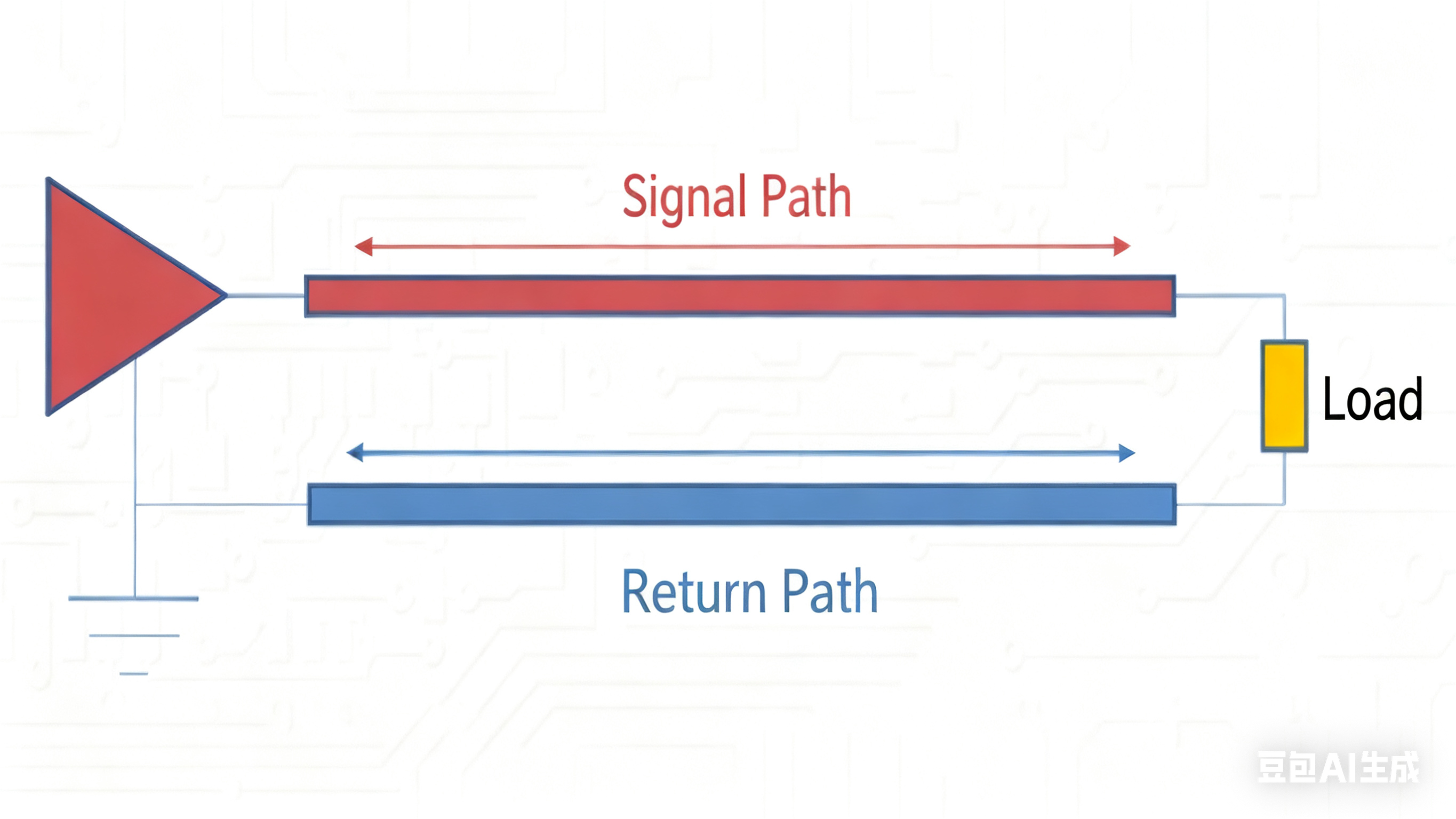
Continuity of Ground Planes and Return Path Optimization
Proper stack-up ensures signal integrity and routing feasibility in compact PCB layouts:
Common Layer Stack-Up Examples
Power and thermal management are among the toughest challenges in compact PCB designs. The smaller the available space, the higher the current density and thermal density become, causing problems to escalate exponentially.
Power Routing
Using Copper for Heat Spreading
Using copper pours for thermal management is one of the most effective methods:
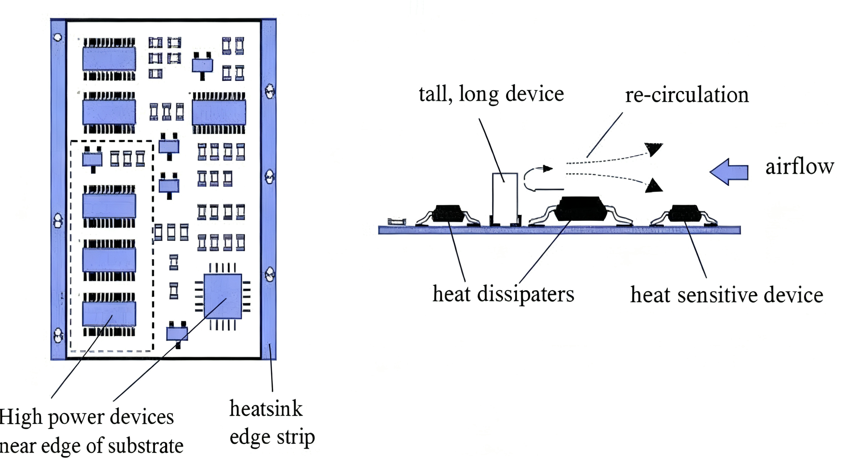
Isolation Between Heat Sources and Sensitive Components
Structural Thermal Features
Silkscreen, Test Points, and Connector Placement
In compact PCB designs, when space is limited, prioritize making component designators (e.g., R1, C5, U3), polarity marks (“+”, “-”, diode cathode line), and Pin 1 indicators clearly readable. Other information, such as project name or version number, can be reduced in size or omitted.
Use the component pads themselves (resistors, capacitors, IC pins) as test points. Ensure these pads are large enough and have sufficient surrounding space for probe access.
Reserve enough clearance around connectors to allow easy finger access for insertion and removal.
Pad Spacing Optimization
This is critical for yield in space-constrained PCB layouts:
The core of compact PCB designs is balancing electrical performance, manufacturability, thermal, and structural requirements within very limited space.
Success in tight-space PCB design relies on proactive planning rather than reactive fixes. From defining constraints and applying effective PCB layout strategies to optimizing the layer stack-up and thermal management, manufacturability (DFM) must remain central.
A well-executed compact PCB layout achieves product miniaturization while ensuring performance, reliability, and yield, offering practical guidance on layout tips for compact PCB designs and how to design PCBs in limited space.
Feel free to ask us if you have any question.


