Flexible circuit design involves many challenges. Flexible PCBs must overcome copper work hardening and fatigue, maintain adequate flexibility, and prevent tearing of the FPC substrate. In Flexible PCB manufacturing, bending radius design is one of the most underestimated factors in flex pcb design guidelines, yet it is also one of the most common causes of failure.
This article systematically explains the design principles, common mistakes, and reliability optimization methods for Flex PCB bending areas, providing practical guidance for robust flex pcb design.
When an FPC is bent, the types of stress acting on each side of the neutral axis are different. The inner side of the curved surface is subjected to compressive stress, while the outer side is subjected to tensile stress. The magnitude of these stresses is related to the FPC thickness and the bending radius. Excessive stress can cause FPC delamination, copper trace cracking, and other failures.
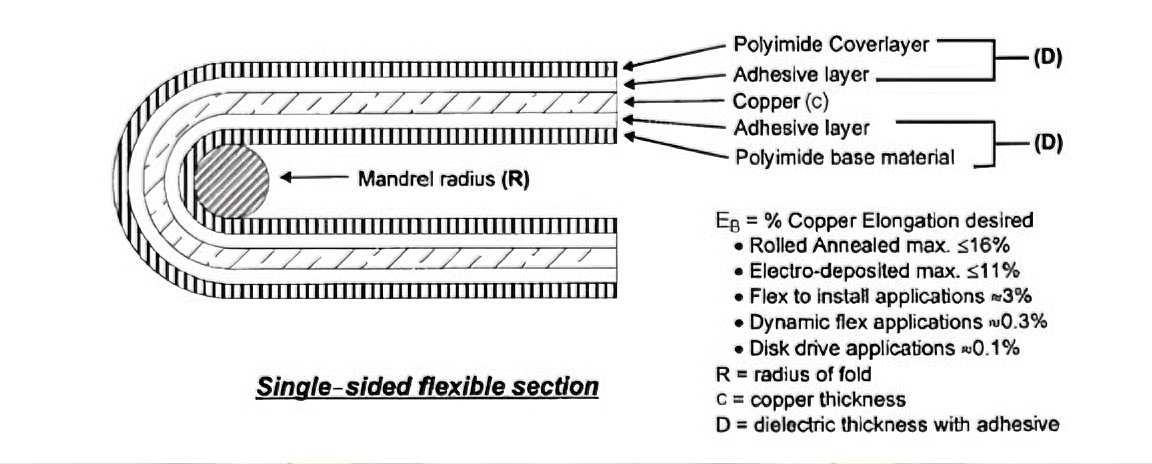
Therefore, during flex pcb design, the FPC stack-up should be arranged so that the layers on both sides of the neutral axis are as symmetrical as possible. In addition, the minimum bending radius should be calculated according to different application conditions, which is a key consideration in flex pcb design guidelines.
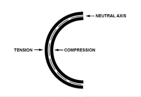
(FPC Bend Stress Diagram)
In design practice, the following formulas can be used to determine the minimum allowable bending radius.
R = Minimum bending radius, μm
c = Copper thickness, μm
D = Dielectric thickness, μm
EB = Copper elongation, %
d = Thickness of the flexible copper-clad dielectric
R = (c / 2) × [(100 − EB) / EB] − D
R = (d / 2 + c) × [(100 − EB) / EB] − D
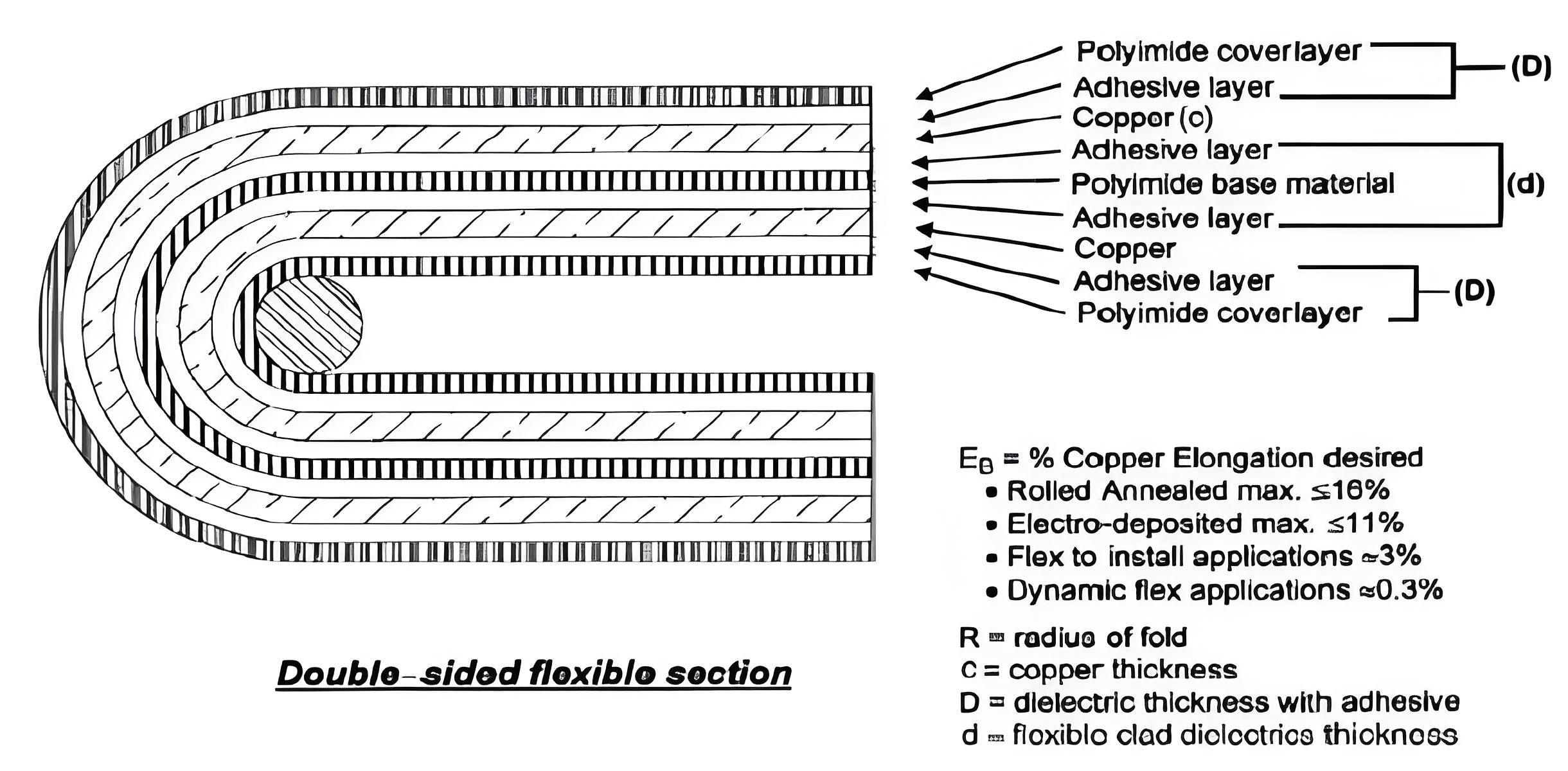
In general practice:
Static bending:
Dynamic bending:
In real-world flex pcb design, it is always better to increase the bending radius rather than reduce the safety margin.
The following designs should be avoided in bending areas:
❌Vias: Their cylindrical structure restricts natural material deformation and often becomes the starting point of delamination.
❌Pads: Solder materials (solder paste, silver paste) and components are inherently rigid, locally “locking” the flexible material and generating tearing stress at the pad edges during bending.
❌Abrupt trace changes: Right-angle or sharp-corner traces, as well as sudden changes in trace width, are natural stress concentration points and are highly prone to copper fatigue cracking.
✅Trace routing should be perpendicular to the bending axis. This is the most important rule.
❌If traces run parallel to the bending direction, repeated bending will continuously compress or stretch the traces.
✅Smooth curved traces are strongly recommended. When length compensation is required, use large-radius, gradual serpentine traces.
❌Right-angle or sharp turns create stress concentration points and can easily lead to trace fracture.
✅Within the bending area, traces should maintain uniform width and spacing to avoid impedance discontinuities.
In addition to layout and routing, the number of layers, material selection, and surface finish choices of flexible PCBs are also critical. For guidance on selecting these parameters, you may refer to this article.
A well-designed flex pcb bending radius not only significantly improves product reliability, but also reduces the risk of rework, scrap, and after-sales issues. If you are working on flexible circuits or rigid-flex PCB design, it is recommended to clearly define the bending areas and bending radius requirements before layout, and to communicate with PCBWay FPC Design in advance to confirm the design details.


