 Mila
Dec 18,2025
4107
Mila
Dec 18,2025
4107
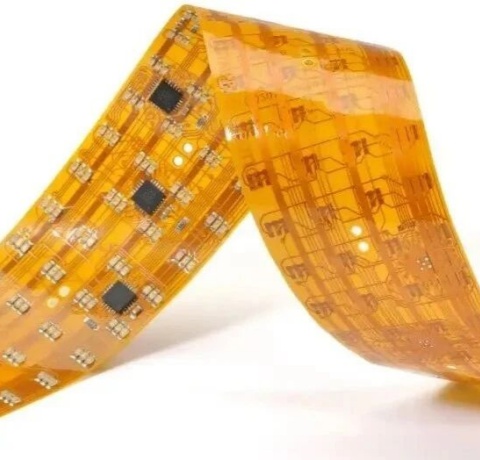
What Determines Flexible PCB Cost: Key Factors Explained
Flexible PCB (FPC), also known as a flexible circuit board, is a type of printed circuit board. However, it differs significantly from traditional rigid PCBs in structure and application, which is why...
Mila
Dec 12,2025
8530
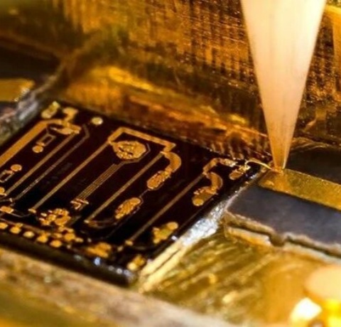
Gold Wire Bonding: Choosing the Right Gold Thickness and Surface Finish
Gold wire bonding is a PCB manufacturing process that uses extremely fine gold wires to connect the leads of a chip or device to PCB pads, electrodes, or lead frames. It is a wire bonding process that...

 Mia
Mar 15,2025
9650
Mia
Mar 15,2025
9650
PCB Flying Probe Test: Principles, Advantages, and Applications
What is PCB Flying Probe Testing?PCB (Printed Circuit Board) Flying Probe Testing (FPT) is an automated method used to test the electrical performance and connectivity of a PCB. Unlike traditional bed...

Mia
Sep 13,2024
18650
ENIG vs. Hard Gold Plating
In the PCB manufacturing process, selecting the appropriate surface finish is crucial to the performance and reliability of the circuit board. Among these, Electroless Nickel Immersion Gold (ENIG) and...

Mia
Aug 21,2024
6761
Solution for Copper Base Discoloration After High-Temperature Furnace: OSP Treatment
In the manufacturing process of copper base PCB, the discoloration of the copper base, which acts as a heat conductor, due to oxidation has always been a significant challenge. During production, if t...

Mia
Jul 10,2024
6433
How should the solder mask color be chosen for color-printed PCBs?
In the process of manufacturing colored printed circuit boards (PCBs), the choice of solder mask color is crucial as it directly relates to the realization of design intentions and the creation of vis...

Mia
Mar 29,2024
20742
Factors that Influencing Prices for PCB Manufacturing and Assembly
In electronic manufacturing, PCBs are vital parts. However, the cost of their manufacturing and assembly is influenced by various factors. From size and materials to specific manufacturing processes u...

Mia
Dec 12,2023
17225
Reasons to Choose SYTECH-S1000H
Choosing the appropriate base material is crucial for the performance and reliability of electronic products. Among the numerous options available, the SYTECH S1000H TG150 board is gaining more and mo...

PCBWay
Mar 10,2023
94647
What is a Fiducial Mark? | PCB Knowledge
What is a Fiducial Mark and How Does it Work?A fiducial mark is typically a circular pad or other shapes of exposed copper that is surrounded by a clearance area. It acts as a reference point for auto...

PCBWay
Oct 17,2022
8696
FQC and Packaging | Multi-layer PCB Manufacturing Process - 16
Final Quality ControlFQC, short for final quality control, is the comprehensive and final inspection of printed circuit boards before shipping to ensure that the boards meet the specifications. Althou...

PCBWay
Oct 07,2022
8785
Electrical Test | Multi-layer PCB Manufacturing Process - 15
After all the manufacturing processes of the circuit board have been completed, the electrical test is carried out to check the board for open circuits and short circuits. The two most commonly used t...

PCBWay
Sep 30,2022
8346
Profile | Multi-layer PCB Manufacturing Process - 14
The process of PCB profile is to cut the production panel into specific sizes and shapes based on the customer's design requirements. To facilitate PCB assembly, the boards can be profiled in individu...

PCBWay
Sep 23,2022
13230
Surface Finish | Multi-layer PCB Manufacturing Process - 13
Bare copper of PCB is easily oxidized by moisture when exposed to air, and the resulting oxide layer of copper has a great impact on the soldering, which may lead to cold soldering and even cause the ...

PCBWay
Sep 19,2022
9856
Legend Printing | Multi-layer PCB Manufacturing Process - 12
Legend printing ,also known as Silkscreen, is a process of printing informational texts or patterns on the surface of the board. Legend information includes component reference designators, switch set...

PCBWay
Sep 15,2022
10193
PCB Surface Finishes
Bare copper has good solderability, but it is easily oxidized by moisture when exposed to air. The oxide layer of copper has a great impact on the soldering. It may lead to cold soldering and even cau...

PCBWay
Sep 09,2022
9358
Soldermask | Multi-layer PCB Manufacturing Process - 11
As a protective layer, the solder mask layer is covered on the traces and substrates that do not need to be soldered to prevent short circuits during soldering. At the same time, it serves to provide ...

PCBWay
Sep 02,2022
9477
Automatic Optical Inspection | Multi-layer PCB Manufacturing Process - 10
AOI - Automatic Optical InspectionDuring the etching process, the etching method, the etching rate, the types and pH value of the etchants, or other factors directly affect the quality of the circuits...

PCBWay
Aug 26,2022
6920
Etching | Multi-layer PCB Manufacturing Process – 09
In the previous step, the copper surface is covered with a layer of tin as an etching resist. Now we need to remove the unwanted copper from the surface to obtain the final desired circuits. This proc...

PCBWay
Aug 19,2022
11039
Pattern Plating | Multi-layer PCB Manufacturing Process - 08
After developing, the copper thickness of the exposed circuits needs to be increased by a secondary copper plating, namely pattern plating. The purpose is to make the hole copper and surface copper of...

PCBWay
Aug 15,2022
8778
Outer Layer | Multi-layer PCB Manufacturing Process - 07
In the previous steps, we have completed the creation of all the inner layer circuits and the required holes (Through/Buried/Blind holes). Next, we have to enter the outer layer imaging process of the...
| Ranking | Name | Answers |
|---|---|---|
| 1 | PCBWay Team | 7 |


