Rigid-Flex PCBs combine rigid circuit boards and flexible circuits into one integrated structure. They include robust rigid areas for component assembly and flexible areas that can bend or fold, with continuous copper layers providing electrical interconnection.
The Rigid-Flex PCB layer stack-up is the core of design and manufacturing, as it directly affects the board structure, electrical performance, and signal integrity.
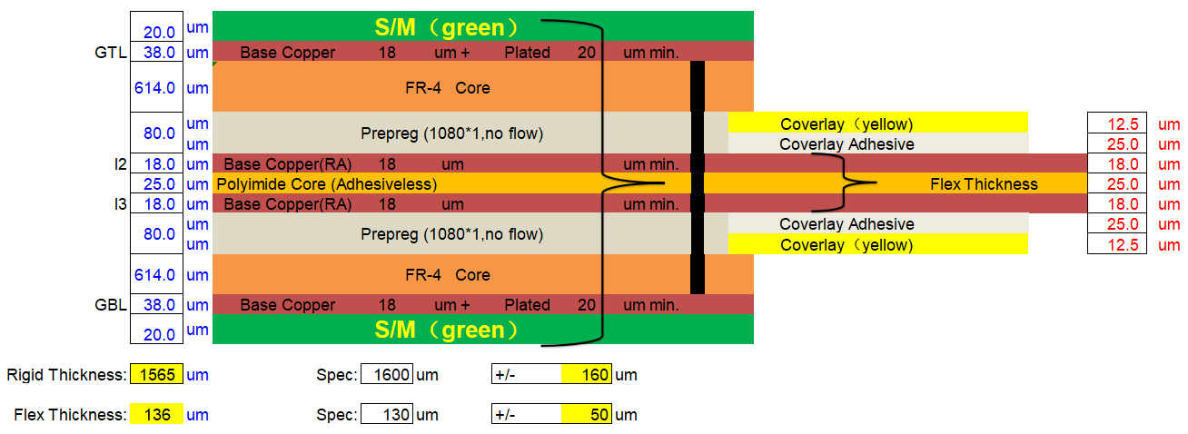
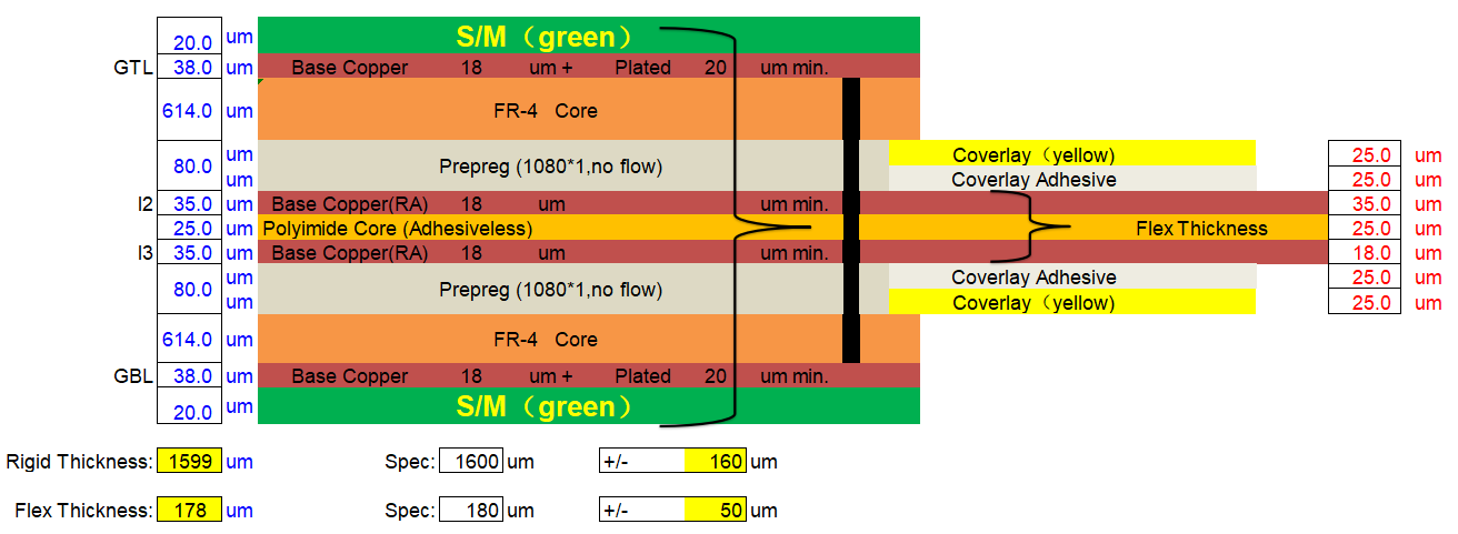
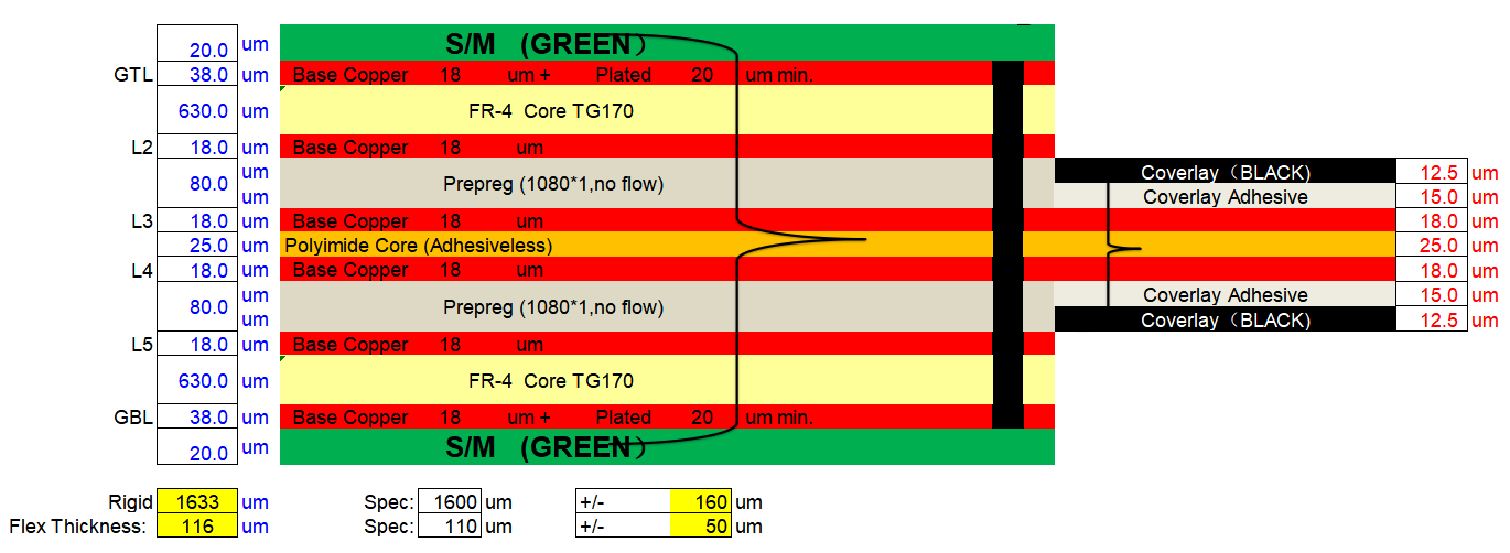
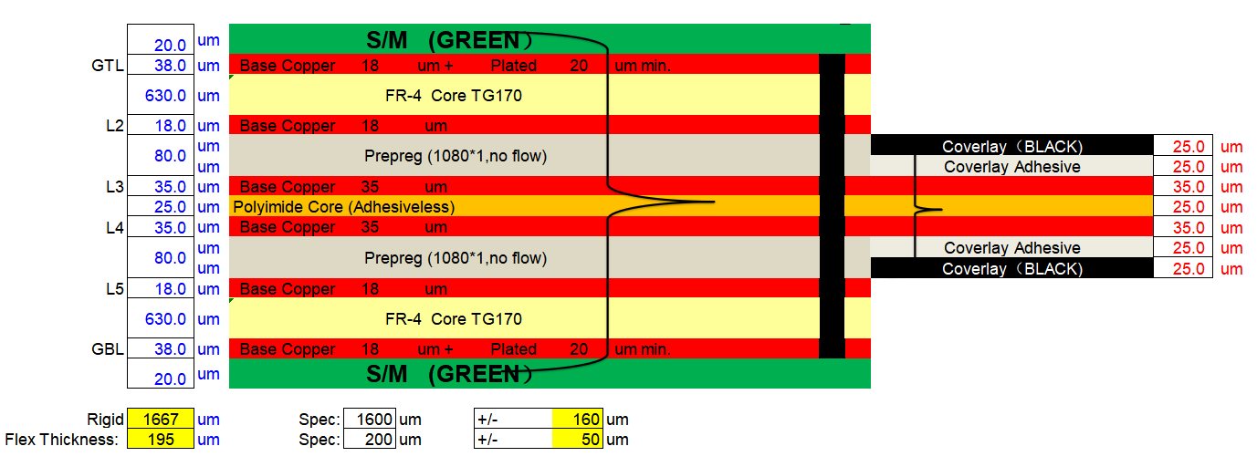
This article introduces typical 4-layer / 6-layer / 8-layer / 10-layer Rigid-Flex PCB stack-up designs.
The rigid sections are based on FR-4 core materials laminated together by prepregs, like glue that bonds the cores during the lamination process. Copper foils are then pressed on each layer to form the circuitry.
The flexible sections use polyimide (PI) base material, clad with copper on both sides, and protected by a coverlay film (not solder mask), making them capable of free bending with no rigid materials inside.
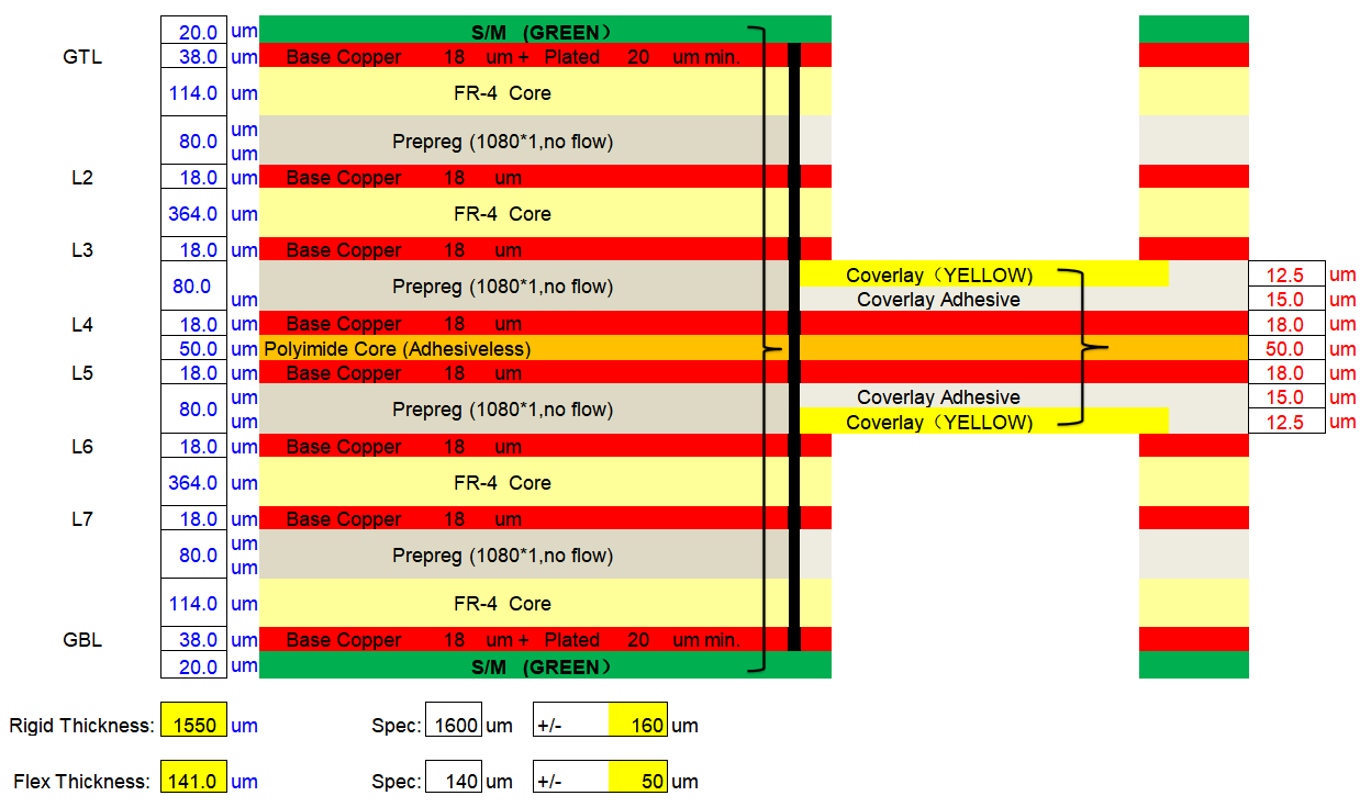
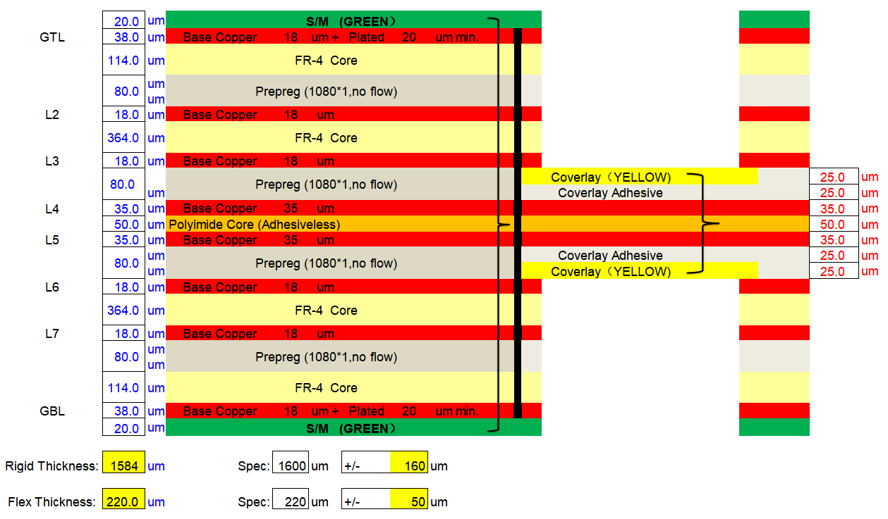
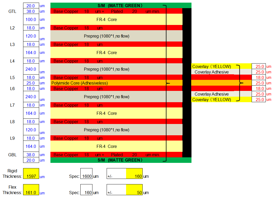
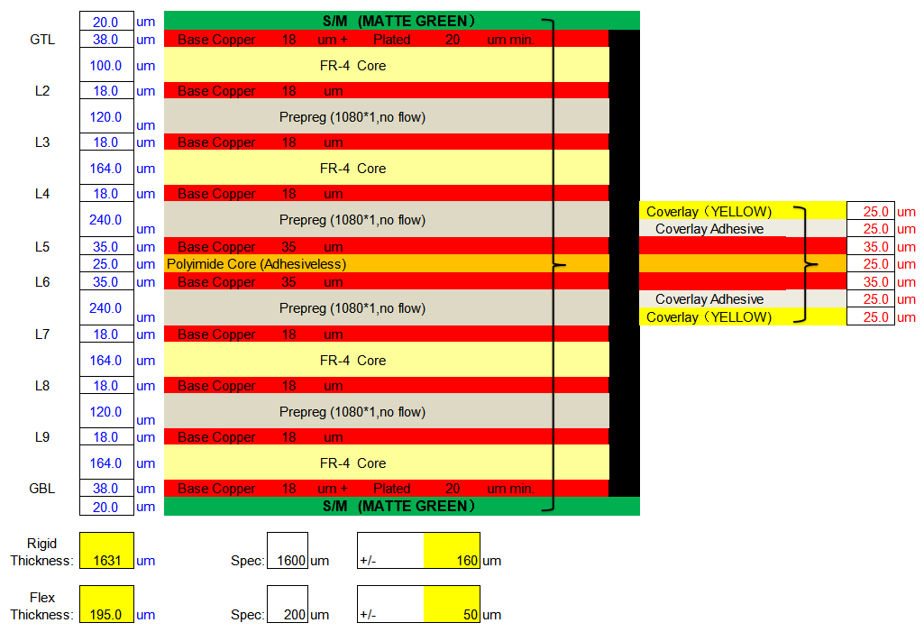
Rigid-Flex PCB layer stack-up is essential to achieving both mechanical durability and electrical performance. We recommend referencing our standard stack-up options during your stack-up design phase for optimal manufacturability.
The article lists only some common laminate configurations. If you’d like to learn more about laminate configurations for rigid-flex boards, please refer to this: Rigid-Flex PCB Standard Stackup
You can learn more about laminate information, including rigid board stack-up and flexible board stack-up, to help you design better.
If you require stack-up of different copper thicknesses, different flex layer, different PCB thickness, please contact your sales representative or our online service for further details.


