 Mila
Sep 16,2025
7390
PCB Layout Design Process from Schematic to Manufacturing
PCB layout design is the process of transforming an electrical schematic into a complete, manufacturable printed circuit board (PCB). A well-designed PCB layout must do more than simply connect compon...
PCBWay
Oct 16,2026
350
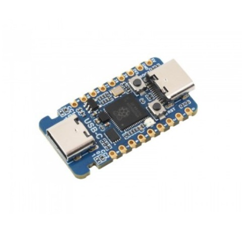
PCBWay Store NewArrival Product - RP2350-USB-C Microcontroller Development Board Based
Link:RP2350-USB-C Mini Development BoardBased on Raspberry Pi RP2350ACastellated module, suitable for SMD applicationsVersion OptionsRP2350-USB-Cwith PIO-USB female port C/C++, MicroPython, ...
Mila
Oct 16,2026
75
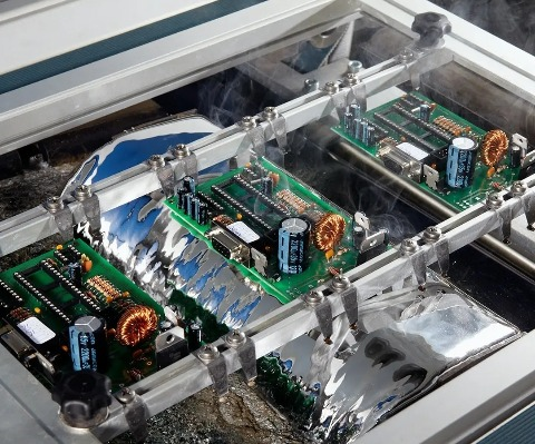
Reflow Soldering vs. Wave Soldering: Key Differences and PCB Design Tips
As hardware engineers, we design the PCB, select the components, and send the Gerber files to the manufacturer. But have you ever wondered why some components go through reflow soldering while others ...
Mila
Oct 15,2026
99
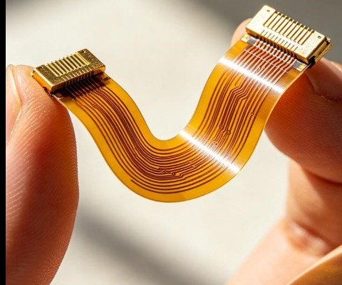
Flex PCB Design Guidelines for Reliable Bending
Unlike rigid PCBs, flexible PCBs (FPCs) can bend and fold to fit into compact electronic devices. They are widely used in smartphones, laptops, printers, and other products where space is limited or c...
Mila
Oct 13,2026
230
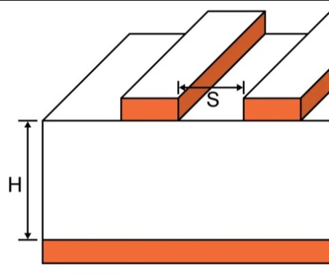
How to Reduce Crosstalk in PCB Routing: Spacing, 3W Rule, and More
Many hardware and PCB layout engineers rely heavily on experience when dealing with crosstalk. Routes that are too close may cause interference, while increasing spacing can make routing difficult. So...
Mila
Oct 12,2026
348
Are More PCB Decoupling Capacitors Always Better?
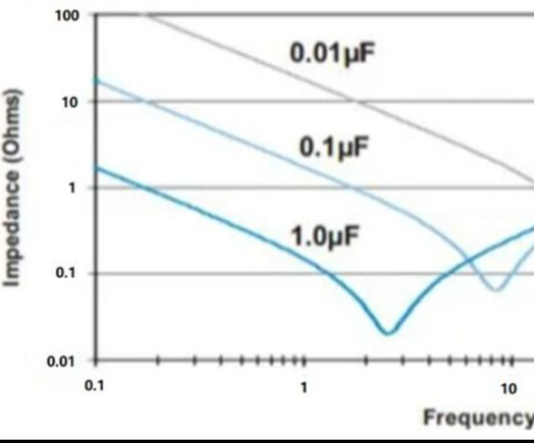
If you have ever designed a PCB schematic, you have probably placed a familiar trio of capacitors near a chip’s power pins: 0.1 µF, 1 µF, and 10 µF.It seems like a safe bet. Different capacitance valu...
PCBWay
Oct 08,2026
982
PCBWay Store NewArrival Product - M5Stack CoreS3 ESP32S3 IoT Development Kit
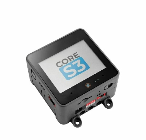
Link:CoreS3CoreS3 is the third-generation main controller of the M5Stack development kit series, based on the ESP32-S3 solution featuring a dual-core Xtensa LX7 processor running at 240 MHz with built...
Mila
Oct 07,2026
543
Why Do PCBs Need Stitching Vias Along the Board Edge?
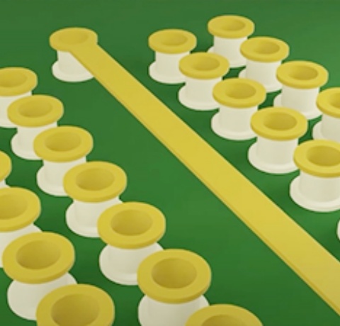
Anyone who has worked on PCB layout has probably experienced this: after finishing the layout, you hand the board over to a senior engineer for review. They take a quick look around the board and ask,...
 MindForge Mechanics
Oct 04,2026
240
HALO Grappleshot - Test Unit 1 Pneumatic Prototype (WIP)
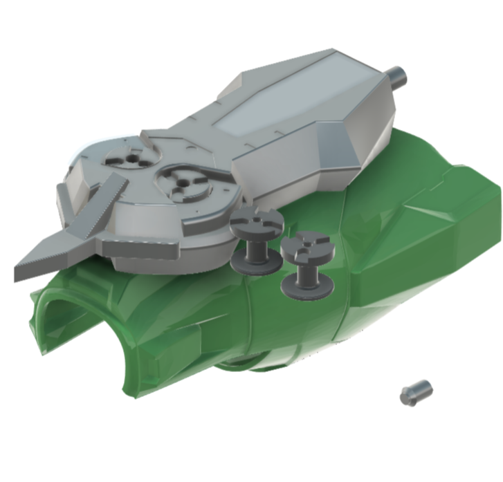
IntroductionThis project is my first full electromechanical prototype of a HALO‑inspired grappleshot, designed for STEM Regionals and built under my maker brand, MindForge Mechanics. Instead of being ...
Mila
Sep 30,2026
265
Analog vs Digital Circuits: Understanding Digital, Analog, and Mixed-Signal Chips
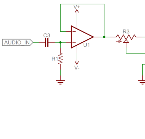
We often say that the world of chips consists of only 0s and 1s. But more accurately, digital circuits use defined voltage ranges to represent discrete logic states, while the real world is clearly no...
PCBWay
Sep 30,2026
578
PCBWay Store NewArrival Product - M5Stack NanoC6 Dev Kit
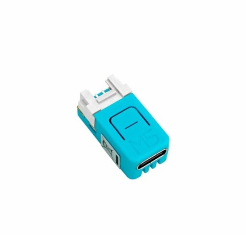
Link:NanoC6NanoC6 is a micro and low-power IoT development board in the M5Stack development kit series. It is equipped with an ESP32-C6FH4 SoC, supporting wireless communication technologies such as W...
Mila
Sep 29,2026
669
Power Supply Design and Layout Guidelines for LDO and DCDC
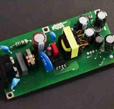
Power supply design is not simply about choosing the right regulator and adding enough copper. The PCB layout directly affects thermal performance, noise, EMI, stability, and overall power integrity.L...
Mila
Sep 29,2026
1281
Threaded Holes in CNC Machining: Thread Types, Depth, and Design Tips
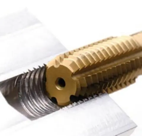
Threaded holes are widely used in CNC machined parts for fastening, assembly, and maintenance. From simple mounting holes to precision mechanical connections, properly designed threads help ensure rel...
Mila
Sep 28,2026
415
How Vias Affect Signal Integrity in High-Speed PCB Design
Anyone involved in high-speed PCB design has probably heard this rule of thumb: minimize vias in high-speed routing whenever possible.But many engineers know they should do this without fully understa...
Mila
Sep 28,2026
495
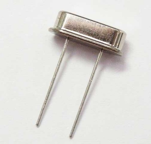
Why No Traces Under a Crystal Oscillator in PCB Layout?
When designing a PCB, many engineers have heard the rule: no traces should run under a crystal oscillator. But why? Can a low-speed signal trace really affect a crystal oscillator? And can a guard rin...
| Ranking | Name | Answers |
|---|---|---|
| 1 | PCBWay Team | 12 |
| 2 | Engineer | 1 |
| 3 | SAAD ZAFAR | 1 |