 Mila
Oct 22,2026
68
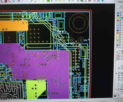
PCB Routing Guidelines for Ground, Power, and Signal Traces
Poor PCB routing can lead to signal integrity issues, EMC failures, and power instability, even when component selection and schematic design are correct. These problems often stem from discontinuous ...
Mila
Oct 13,2026
345
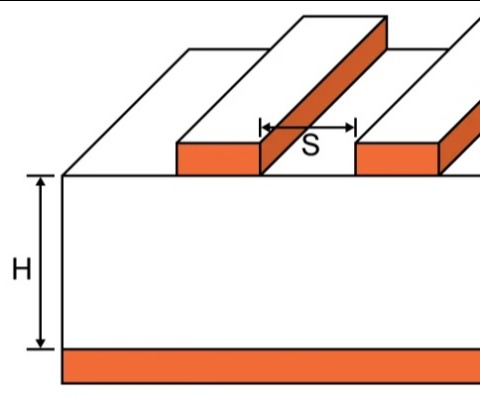
How to Reduce Crosstalk in PCB Routing: Spacing, 3W Rule, and More
Many hardware and PCB layout engineers rely heavily on experience when dealing with crosstalk. Routes that are too close may cause interference, while increasing spacing can make routing difficult. So...
Mila
Sep 28,2026
565
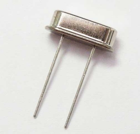
Why No Traces Under a Crystal Oscillator in PCB Layout?
When designing a PCB, many engineers have heard the rule: no traces should run under a crystal oscillator. But why? Can a low-speed signal trace really affect a crystal oscillator? And can a guard rin...
Mila
Sep 02,2026
401
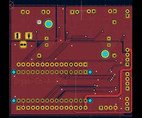
PCB Routing Angle Rules and the 90 Degree Trace Myth
In the realm of hardware design, "never use 90° angle traces" is one of the most widely circulated rules. Most engineers habitually modify 90° corners into 45° bends, or even intentionally increase tr...

Mila
Aug 27,2026
827
PCB Routing Layer Selection for High-Speed Signals: Microstrip vs. Stripline
In the hardware layout for high-speed interfaces such as PCIe, DDR5, USB 3.0, and SerDes, selecting the trace layer—specifically choosing between surface microstrip and inner stripline—is a core decis...
Mila
Nov 07,2025
5378
PCB Layout Design Guidelines: Placement and Routing
Overview of PCB Layout and RoutingIn PCB design, layout is a critical stage that directly determines the quality of the routing. A well-organized layout ensures efficient signal paths and reliable pow...

 Mia
Jul 17,2024
27592
PCB Design Layout Guidelines for Routing
1. Length Control in RoutingLength controlling is very important in PCB design. The traces should be kept as short as possible to avoid introducing unnecessary interference due to excessive length. Fo...
 Karen Lin
May 19,2014
5602
Minimize crosstalk with optimized PCB routing technique
I. IntroductionToday, there are a number of high speed digital communication protocols applied in portable computing devices with compact PCB dimensions. Protocols such as PCIe, USB, and SATA have dat...
Karen Lin
Apr 14,2014
3933
PCB and Routing Solutions: Centering Traces in BGA
To increase fabrication yield, it is important to center the traces between the fanout vias inside the BGA area. Large BGAs are usually 1mm pitch and medium sized ones are 0.8mm. Then we go down to 0....
Karen Lin
Apr 10,2014
2583
PCB and Routing Solutions: Introduction
My name is Charles Pfeil and my role at Mentor Graphics is one in which I always have a primary focus on routing technology and methods – although I do get involved in numerous other projects. I began...
Karen Lin
Mar 12,2014
3147
PCB Routing Techniques
printed circuit board (PCB) routing techniques are a bit like a piece of artwork. There is an engineering component -- the load of various circuit and solder paths cannot intersect or interfere with t...
PCBWay
Dec 10,2013
7055
Custom PCB shapes
In business as in life, we learn more from listening than talking. We may think our message is getting out but just because we understand our processes completely, doesn’t mean our customers do. The ...
PCBWay
Dec 10,2013
1806
Remote testing fast 40 a DC/DC controller correction of the output voltage error caused by PCB routing
Ling (Linear Technology) the company launched two phase step-down LTC3709 type synchronous DC/DC controller, the device has a fast transient response, can eliminate caused by PCB routing and big load ...
| Ranking | Name | Answers |
|---|---|---|
| 1 | PCBWay Team | 5 |
| 2 | Kieu Vu | 1 |
| 3 | SAAD ZAFAR | 1 |


