Anyone who has worked on PCB layout has probably experienced this: after finishing the layout, you hand the board over to a senior engineer for review. They take a quick look around the board and ask, “Where are the ground vias along the edge?”
At first, this may seem unnecessary. After all, the board edge does not carry signal traces. So why are stitching vias placed there?
The answer lies in what happens around the edge of a PCB. Properly placed grounding vias can help control electromagnetic coupling, provide a more continuous high-frequency return path, and improve PCB edge shielding. For high-speed, RF, and EMI-sensitive designs, that simple row of vias can make a noticeable difference.
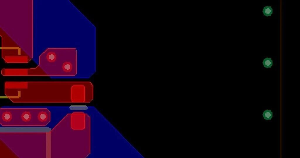
(Stitching Vias)
This row of vias is commonly known as a ground via fence, via fence, or stitching vias.
It is not simply a matter of placing a row of vias around the board. Instead, the vias connect ground structures on different PCB layers and create a more continuous electromagnetic boundary along the board edge.
For high-speed, RF, and high-reliability PCBs, the main benefits include improving high-frequency return paths, reducing electromagnetic leakage and coupling, and enhancing the continuity of local shielding structures.
The PCB edge is the boundary between copper, dielectric material, and air. When high-speed, clock, or RF signals pass through the board, relatively strong electromagnetic fields may exist around this region.
If the reference ground structure around the PCB edge is discontinuous, electromagnetic fields can couple outward through the edge, increasing EMI risks. External interference can also couple into sensitive circuits through the same region.
A continuous row of grounding vias creates a low-impedance grounding boundary around the PCB edge.
It can help limit the spread of electromagnetic fields around the edge and reduce coupling between the signals and the surrounding environment, improving EMI performance.
High-speed signal return current generally follows a path close to the signal trace and its reference plane.
When a PCB contains multiple ground or reference planes, insufficient connections between these planes can force high-frequency return currents to take longer paths, increasing both return path length and loop area.
Stitching vias can provide low-impedance connections between different ground layers, giving high-frequency currents a more continuous return path.
The more continuous the return path, the smaller the loop area can be, making electromagnetic radiation and crosstalk easier to control.
For RF, microwave, and high-speed clock PCBs, discontinuities around the board edge can create additional electromagnetic coupling paths and, at certain frequencies, may contribute to unwanted resonance.
A continuous row of grounding vias can improve the electromagnetic boundary conditions around the PCB edge, reduce edge coupling, and help suppress local resonance.
This is particularly useful in RF regions, shielding areas, and areas with dense high-speed signals, where a properly designed PCB ground via fence can be more effective than simply adding more copper.
RF modules and high-speed precision modules often use metal shielding cans.
In this case, grounding vias can work together with the shielding-can solder pad to create a more continuous low-impedance grounding path around the shield.
If a shielding can has only a few grounding points, the parasitic inductance of the connection path can affect high-frequency shielding performance. Adding stitching vias around the shielding-can edge can shorten the high-frequency current path and reduce electromagnetic leakage around the shield.
Therefore, a via fence around a shielding can is generally more suitable for high-frequency shielding than a single-point ground connection.
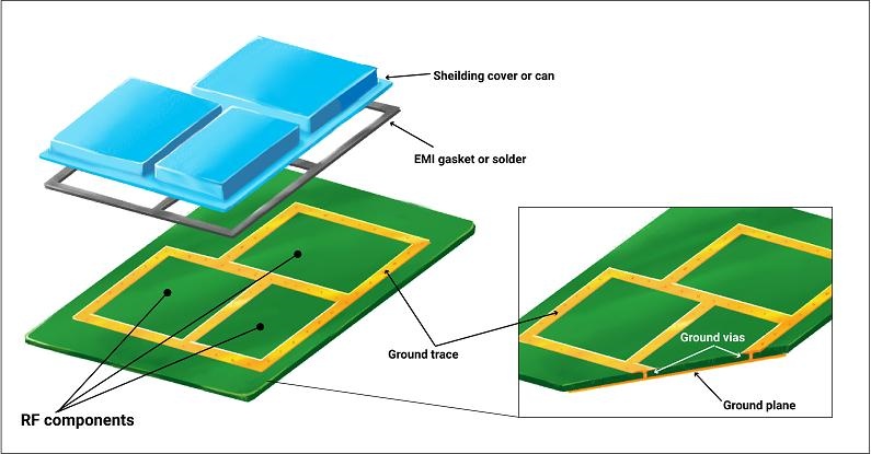
(EMI shielding + stitching vias)
Many engineers think of the grounding vias around a PCB edge as a small Faraday cage.
There is some truth to this analogy, but an important point should be noted: a PCB via fence is not an ideal, completely enclosed Faraday cage.
The basic idea behind a Faraday cage is to use a continuous conductive structure to shield against electromagnetic fields through reflection, absorption, and boundary effects.
On a PCB, continuous ground copper, reference planes, stitching vias, and metal shielding cans can work together to create a similar shielding structure.
One important function of the grounding vias is to connect ground structures on different layers and reduce electromagnetic “openings” around the PCB edge.
At high frequencies, shielding effectiveness depends on many factors, including conductor continuity, via spacing, opening size, material, operating frequency, and the overall structure.
Therefore, instead of simply applying a fixed wavelength ratio, the via spacing should be determined based on the actual operating frequency, signal rise time, and PCB structure.
For high-speed digital signals, the relevant frequency content is not necessarily equal to the clock frequency. Signal rise time also needs to be considered.
Limitations
The effectiveness of the shielding structure also depends on the PCB reference planes, return paths, connectors, shielding cans, and other design elements.
Adding vias around the board is not simply a matter of placing them in a row. Via spacing, location, grounding method, and edge copper design all need to be considered according to the actual PCB structure. Here are some common design principles.
A common engineering approach is to estimate the via spacing based on the wavelength corresponding to the target frequency. For example, λ/10 or a smaller spacing can be used as an initial reference.
However, this is not a fixed standard that applies to every PCB.
Actual design should also consider:
For ordinary PCBs, relatively wider via spacing may be sufficient. For high-speed, RF, or high-EMI areas, the spacing may need to be reduced.
Common engineering reference values include:
Do not mechanically apply a fixed value. The final via spacing should be determined based on the actual frequency and structure.
Edge grounding vias should maintain an appropriate clearance from the PCB outline.
Sufficient clearance should be provided according to the PCB manufacturer's fabrication capability to prevent damage to the vias during routing, milling, V-cut, or other board-edge processing.
At the same time:
It is important to note that not every ground plane needs to be connected through the same via. The exact connection method should be determined based on the PCB stackup and return-current path.
Many designers add a row of vias but overlook the ground copper between them.
This alone cannot create a complete PCB ground via fence.
A continuous ground copper area should be provided around the PCB edge according to the board structure, with grounding vias connecting it to the internal reference ground plane.
The vias provide vertical connections, while continuous ground copper provides horizontal connections. Together, they form a more complete grounding boundary.
High-speed signal traces, slots, or other structures should not arbitrarily cut through this grounding boundary.
The entire PCB does not necessarily need the same via spacing.
The following areas may require additional stitching vias:
Board-edge connectors and interfaces:
Connectors are important paths through which external signals enter the PCB. Proper grounding vias can improve the return path around the interface and reduce edge coupling.
Shielding-can areas:
Dense grounding vias around the shielding-can solder pad can create a more continuous high-frequency grounding path.
RF and high-speed clock areas:
For areas that are particularly sensitive to EMI or crosstalk, reducing the via spacing can strengthen local shielding.
Proper stitching vias are an important part of high-speed PCB layout and PCB design.Their core function is to improve high-frequency return paths around the PCB edge and reduce electromagnetic coupling and EMI leakage through the combination of stitching vias and continuous reference-ground structures.
For high-speed, RF, and EMI-sensitive PCBs, proper PCB via stitching and PCB edge shielding are particularly important.
But remember: more vias are not always better, and not every PCB needs a dense row of grounding vias. Via spacing, edge clearance, reference planes, and local shielding structures should all be determined based on the actual signal frequency, rise time, and PCB stackup.