If you have ever designed a PCB schematic, you have probably placed a familiar trio of capacitors near a chip’s power pins: 0.1 µF, 1 µF, and 10 µF.It seems like a safe bet. Different capacitance values, neatly arranged, ready to keep the power supply stable and suppress noise. But is this tried-and-tested combination always the best choice?
When it comes to decoupling capacitors, does adding more always mean better performance? Not necessarily. Effective decoupling depends on more than capacitance alone. Component characteristics, parasitic effects, and PCB layout all play a role.
Circuit theory tells us that the impedance of an ideal capacitor decreases as frequency increases. Real capacitors, however, are not quite so simple. They have two important parasitic parameters: equivalent series resistance (ESR) and equivalent series inductance (ESL).
ESL deserves particular attention. As frequency increases, the capacitive impedance decreases until the capacitor reaches its self-resonant frequency (SRF). Around this frequency, the capacitor typically exhibits its minimum impedance. Beyond SRF, parasitic inductance begins to dominate, and impedance increases with frequency.
In other words, a capacitor does not become more effective at filtering noise simply because the frequency keeps rising. Above its SRF, its ability to suppress higher-frequency noise may be limited.
That is why selecting a PCB decoupling capacitor requires more than checking its nominal capacitance. You also need to understand how its impedance changes with frequency.
Capacitors with different capacitance values have different impedance characteristics. When selected appropriately, they can help maintain low impedance across a wider frequency range in the power distribution network (PDN).
Each has its strengths, and combining them can make sense.
However, 10 µF, 1 µF, and 0.1 µF are not a universal combination with three fixed frequency ranges. Their effective operating ranges may overlap, and the appropriate values depend on the chip’s requirements, component characteristics, and PCB layout.
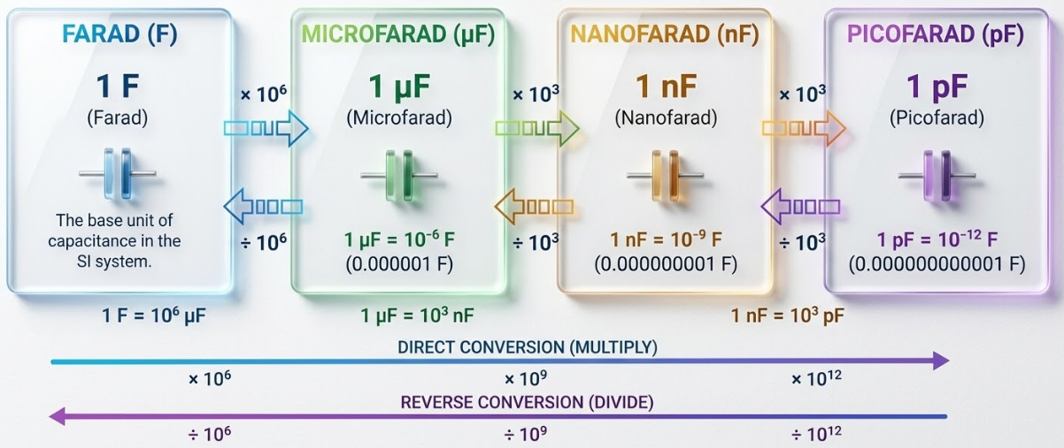
(capacitor unit conversion chart)
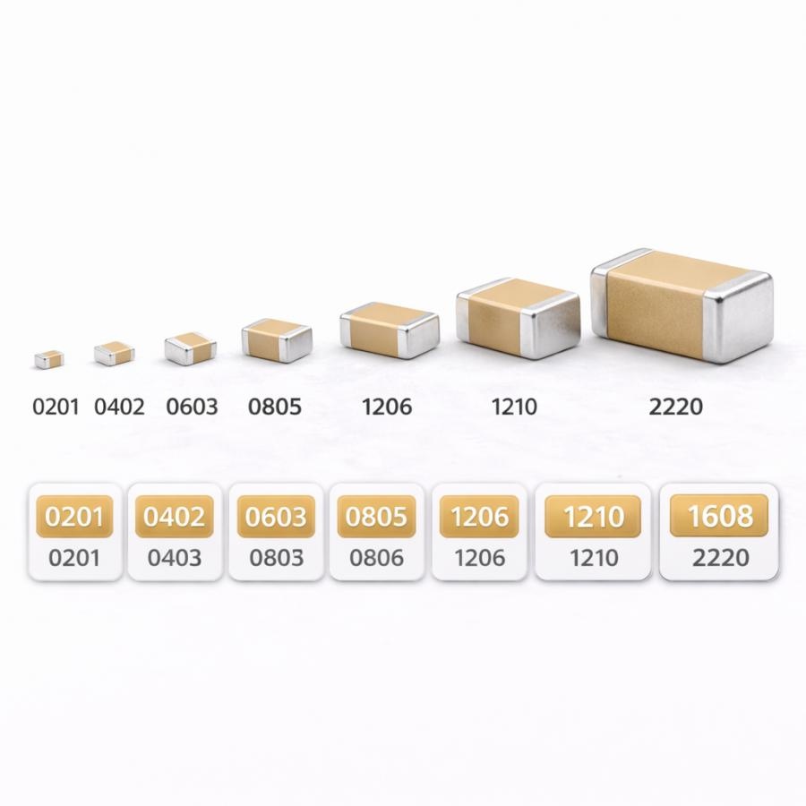
(MLCC Package Size and Decoupling Performance)
Two factors that deserve more attention than capacitance alone are dielectric material and package size.
Let's start with the dielectric. Suppose you choose a 10 µF ceramic capacitor with a Y5V or Z5U dielectric because it is inexpensive and offers the desired nominal capacitance. Once operating conditions come into play, its capacitance may change significantly with temperature and DC bias voltage.
That does not mean these dielectric types are unsuitable for every application. However, their characteristics may make them less suitable for decoupling applications that require stable capacitance.
For common power supply decoupling applications, X7R and X5R are often preferred dielectric types. But choosing either one does not guarantee that the nominal capacitance will be available under operating conditions. Multilayer ceramic capacitors (MLCCs), especially those with high capacitance in small packages, can experience significant capacitance loss under DC bias.
Always check the manufacturer's datasheet, particularly the DC bias curve, to determine how much effective capacitance remains at the actual operating voltage.
For example, a nominal 10 µF X5R capacitor may provide substantially less capacitance at a particular operating voltage and package size. Even if several capacitors are installed, the effective decoupling capacitance may still be insufficient.
Now, let's look at package size. Two 0.1 µF capacitors in 0402 and 0805 packages may have different parasitic characteristics and high-frequency performance.
Under otherwise comparable conditions, a smaller package can help reduce component parasitics and the inductance of the mounting loop. However, the actual improvement depends on the component structure, terminal design, and PCB layout. You cannot assume that ESL decreases by a fixed percentage every time the package size is reduced.
Sometimes, optimizing the package size and mounting loop can be more effective than simply increasing capacitance.
That said, smaller is not always better. Capacitance requirements, voltage rating, soldering reliability, and manufacturing constraints must also be considered.
Some designers assume that if capacitors with different values can cover different frequency ranges, adding more of them should suppress noise across the board.
That sounds reasonable in theory, but reality is more complicated.
When multiple capacitors are connected in parallel, their capacitance, ESR, ESL, and PCB interconnect parasitics interact to form a complex impedance network. Under certain conditions, this network can produce an anti-resonance peak, causing the impedance of the power distribution network to rise at a particular frequency.
In simple terms, some capacitor branches may behave capacitively while others behave inductively at that frequency. Their interaction, together with interconnect parasitics, can create an impedance peak.
The peak's frequency and magnitude depend on the component parameters, connection topology, PCB power planes, and mounting loops. Simply adding or removing capacitors does not guarantee a solution.
PCB space is also limited. Adding too many capacitors can crowd routing areas and force some components farther away from the chip's power pins. Longer connection paths can increase loop inductance and weaken high-frequency decoupling performance.
So, do not focus only on how many capacitors appear in the schematic. Where they are placed, how they are connected, and how the overall network behaves are equally important.
Consider a design example.
Suppose a simulation of an FPGA power distribution network reveals a pronounced anti-resonance peak. Adding more capacitors with different capacitance values may not solve the problem and could even make the peak more pronounced.
A better approach is to examine the impedance curve, analyze the capacitors' ESR and ESL, evaluate interconnect parasitics, and review the layout. The capacitor combination and connection topology can then be adjusted as needed.
In some cases, a more optimized design may use fewer capacitors. However, removing capacitors without checking the impedance response can also increase impedance in certain frequency ranges.
The real goal is not to minimize the number of capacitors, but to optimize the impedance of the entire power distribution network.
It comes down to three key principles.
For high-speed digital circuits, the target impedance method can help guide decoupling design:
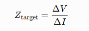
Here, (Delta V) is the allowable power supply voltage variation, and (Delta I) is the transient current change that the power distribution network must support.
First, determine the allowable voltage variation based on the chip's power requirements. Then estimate the target impedance and evaluate the required capacitance values, capacitor count, and placement based on the load's transient behavior and the PDN impedance profile.
Of course, target impedance is only one part of the design process. Voltage regulator response, chip packaging, PCB power planes, and the actual capacitor characteristics must also be considered.
Rather than copying a fixed capacitor combination, start by understanding what the circuit actually needs.
A decoupling capacitor should be placed as close as practical to its corresponding chip power pin. The current loop between the power pin, capacitor, and ground plane should be kept short.
Connect the capacitor's ground terminal to a continuous ground plane through a via placed as close to the ground pad as practical. For high-frequency decoupling, multiple ground vias may help reduce loop inductance, depending on the layout and current path. However, two vias are not mandatory in every design.
Also, proximity alone does not guarantee a good layout. Poor power routing, an indirect ground path, or an unsuitable via connection can still introduce significant parasitic inductance.
Remember: High-frequency decoupling is not just about placing a capacitor close to the chip. It is about creating a short, low-inductance current loop.
This is one of the most important considerations in decoupling capacitor placement and effective PCB layout.
Not every chip needs the full 0.1 µF, 1 µF, and 10 µF combination.
For low-speed circuits with modest transient current demands, a small number of decoupling capacitors may be sufficient, provided the device requirements are met. High-speed FPGAs, processors, and other devices with demanding transient loads may require a more complex capacitor network and a carefully designed power distribution system.
The appropriate number and values of capacitors should be determined using the chip manufacturer's recommendations, target impedance, and design verification results.
A well-designed network is more reliable than a collection of capacitors added without a clear purpose.
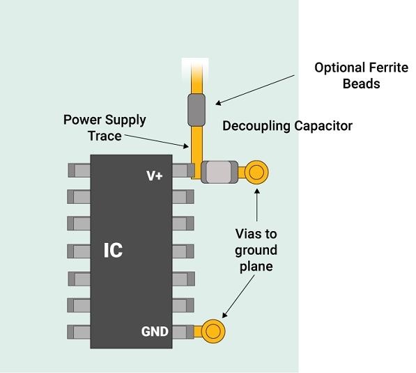
(Good vs. Poor Decoupling Capacitor Placement)
The 0.1 µF, 1 µF, and 10 µF combination is a useful engineering starting point, not a universal rule.
There is a sound reason behind it: capacitors with different capacitance values have different impedance characteristics, and a suitable combination can improve power distribution network performance across different frequency ranges. But that does not mean more capacitance is always better—or that fewer capacitors automatically make a better design.
Good power supply design is not about how many capacitors you solder onto a board. It is about understanding frequency, impedance, component characteristics, and PCB layout.
Do not simply copy a reference design and place capacitors without understanding why they are there. Learn to evaluate the actual requirements and make informed design decisions.
Sometimes, the problem is not that you need more capacitors. It is that the wrong capacitor was selected—or the first one was placed incorrectly.
Less guesswork, more deliberate design. That is the principle behind effective decoupling capacitor selection and PCB power integrity.



