Engineers often encounter hard-to-spot issues when debugging switch-mode power supplies, DC-DC converters, and LDO circuits. These issues typically stem from placing electrolytic or tantalum bulk capacitors alongside 0402 or 0603 small ceramic capacitors arbitrarily.
Symptoms include high power supply ripple, significant voltage sags during load transients, timing anomalies in high-speed ICs, and ADC sampling noise drift. Incorrect placement degrades power performance and expands high-frequency current loop areas, elevating EMC risks.
While parallel configurations of bulk and ceramic capacitors are common knowledge, their spatial placement rules are frequently misunderstood. Below is a breakdown of layout principles based on capacitor impedance characteristics and Power Distribution Network (PDN) design.
1.Power Ssupply Capacitor Differences: Bulk vs. Ceramic Capacitors
A capacitor’s behavior in a power network depends not only on capacitance, but also on Equivalent Series Resistance (ESR), Equivalent Series Inductance (ESL), Self-Resonating Frequency (SRF), and PCB parasitics.
Bulk Capacitors (Electrolytic / Tantalum, μF to mF ange)
- Store large amounts of charge to handle low-frequency load current changes and suppress low-frequency voltage fluctuations.
- Larger packages introduce higher lead ESL. Above their SRF, they exhibit inductive properties and lose low impedance at high frequencies.
Small Ceramic Capacitors (nF to μF range)
- Low ESL MLCCs maintain low impedance at higher frequencies, making them ideal for suppressing MHz switch noise and high-frequency transient interference.
- High-frequency performance is sensitive to trace parasitics; excessively long traces negate their low ESL advantage.
Note: Operating bands cannot be defined solely by capacitance. A 10μF MLCC may outperform a 100μF electrolytic capacitor at high frequencies due to lower ESL. Effective capacitance in MLCCs is also reduced by DC bias, operating temperature, and voltage.
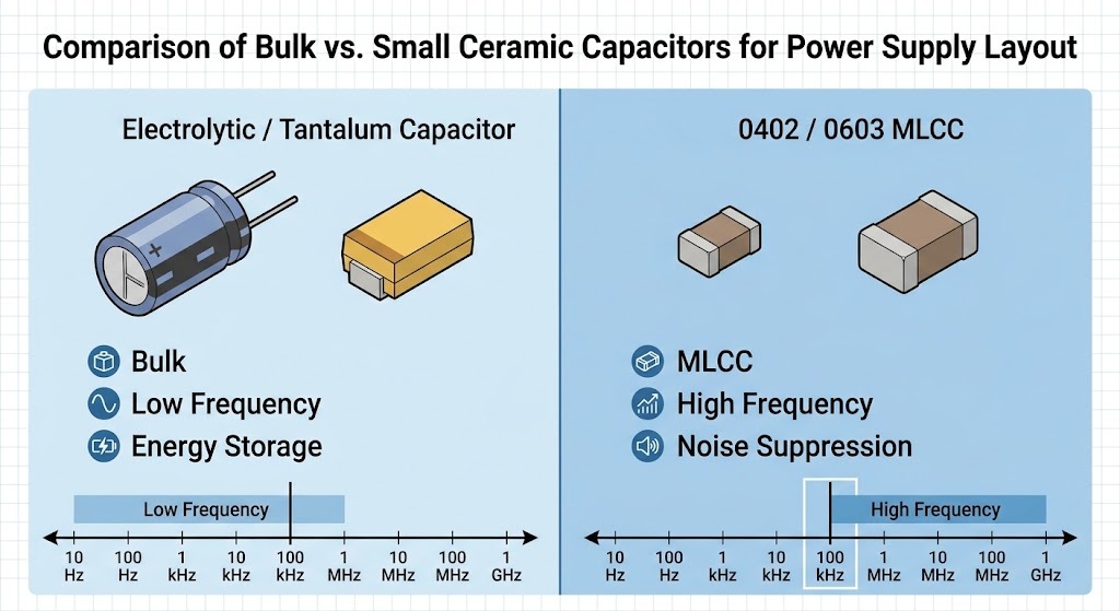
(Bulk Capacitor vs. Small Ceramic Capacitor)
2.Core Capacitor Layout Principles: Lowering PDN Impedance and Parasitics
Connecting capacitors in parallel does not mean current flows through one before reaching the other. The goal of a Power Distribution Network is to keep PDN impedance (ZPDN) below a target threshold: ZPDN = Vnoise/ Itransient
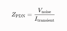
Lower PDN impedance reduces voltage noise (Vnoise) during transient current spikes (Itransient). At lower frequencies, trace inductive reactance (XL = 2π f L) remains minimal, allowing bulk capacitors to supply charge even when placed further away.
As frequency rises, parasitic inductance grows rapidly. Proper decoupling capacitor placement demands placing low-ESL ceramic components as close to the IC power pins as possible to minimize loop area and lower high-frequency impedance.
Key High-Frequency Loops:
- IC Decoupling Loop: IC Power Pin → MLCC → GND → IC GND Pin.
- DC-DC Power Loop: High di/dt loops formed by switching elements, input bypass capacitors, power inductors, and return paths.
Optimizing capacitor layout requires prioritizing high di/dt loops in DC-DC converters, while IC decoupling requires shortening the supply and return paths between the load and the MLCC.
- Placement Rule: Position low-ESL ceramic capacitors closest to IC power pins. Place bulk energy storage capacitors near power inlets or DC-DC/LDO output pins.
- Converter Exceptions: DC-DC output capacitors are part of the control loop and power filter. They must strictly follow datasheet requirements and sit near converter pins. LDO capacitors must also strictly align with datasheet ESR and placement specifications.
- Routing: Avoid routing traces serially from bulk to small capacitors and then to the IC pin, as this lengthens the high-frequency loop. Connect both capacitors directly to the power plane with short traces.
3.Practical Capacitor Placement Guidelines
- DC-DC and LDO Input Placement: Place bulk capacitors at the input for local energy storage and low-frequency ripple suppression based on datasheet recommendations. Position low-ESL ceramic capacitors directly adjacent to the VIN pin.
- DC-DC and LDO Output Placement: Prioritize datasheet guidelines for output power supply capacitor selection. Place small ceramic capacitors close to converter VOUT pins or load IC pins to suppress switching noise. Minimize Buck converter power loop areas.
- Proximity Rule for Small Ceramic Capacitors: Shorten both power and GND current paths. A short power trace paired with a long return path degrades high-frequency decoupling.
- Low-Impedance Grounding: Connect capacitor GND terminals to a continuous reference plane using short, low-inductance paths. Place GND vias directly adjacent to component pads.
- Multi-Stage Filtering: Avoid mechanically sorting capacitors strictly by size and distance. Place bulk capacitors near power inputs and low-ESL MLCCs near sensitive loads. When adding ferrite beads for multi-stage filtering on sensitive rails (e.g., ADC or RF), evaluate potential impedance resonances between the bead and adjacent capacitors.
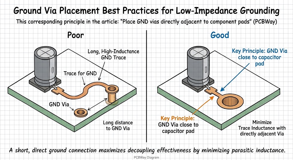
(Good vs. Poor Ground Via Placement)
4.Power Supply Capacitor Layout Checklist
- Place low-ESL ceramic decoupling capacitors closest to IC power pins.
- Follow datasheet specifications for DC-DC and LDO input/output capacitor parameters and layout.
- Avoid serial routing that forces current sequentially through capacitors.
- Keep power and ground traces as short as possible to minimize high-frequency loop areas.
- Connect capacitor ground terminals with short paths and vias adjacent to pads.
- Minimize high di/dt power loop areas in DC-DC converters.
- Ensure LDO output capacitor ESR falls within the specified stability range.
- Validate multi-stage filter layouts against PDN impedance targets rather than relying on basic capacity-to-distance rules.