Power supply design is not simply about choosing the right regulator and adding enough copper. The PCB layout directly affects thermal performance, noise, EMI, stability, and overall power integrity.
LDOs and DCDC converters have different layout priorities: LDOs require careful attention to heat dissipation, capacitor placement, and power loss, while DCDC converters are more sensitive to high-frequency current loops, feedback routing, and grounding. When both are used in the same system, power-stage isolation and decoupling become equally important.
In this guide, we’ll break down the key power supply layout considerations and common mistakes for LDOs, DCDC converters, and mixed power architectures.
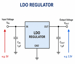
(LDO regulator)
Advantages: Low noise, no switching interference, and simple peripheral circuitry
Disadvantages: Efficiency depends on the input-to-output voltage difference, and large voltage drops or high load currents can generate significant heat.
Mistake 1: Poor Thermal Management → Excessive Temperature Rise
Incorrect: Leaving the exposed pad floating without sufficient copper area or thermal vias.
Consequence: Higher thermal resistance can increase junction temperature, potentially triggering thermal protection or affecting long-term reliability.
Correct:
Mistake 2: Input/Output Capacitors Too Far from the Pins → Reduced Stability and Transient Performance
Incorrect: Placing the input and output capacitors far away from the LDO pins.
Consequence: Increased parasitic impedance can affect stability, transient response, and high-frequency noise performance.
Correct:
Mistake 3: Ignoring Voltage Drop and Power Dissipation → Efficiency and Thermal Issues
Incorrect: Using an LDO for high input voltage and high current without evaluating power dissipation.
Consequence: Higher LDO power dissipation increases junction temperature and may trigger thermal protection or reduce system reliability.
Correct:
The main power dissipation of an LDO can be estimated using: P ≈ (Vin − Vout) × Iout
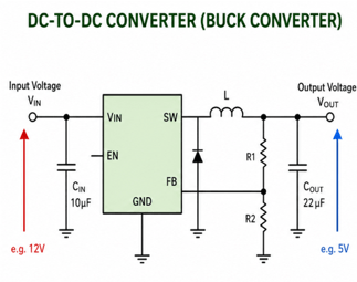
(dc-dc converter)
Advantages: High conversion efficiency, higher output current capability, and suitability for a wide range of input and output voltages
Disadvantages: Switching nodes and high di/dt currents can generate noise, making DCDC PCB layout critical to EMI, stability, and overall power performance.
Mistake 1: Long Power Loops → Increased Ringing and EMI
Incorrect: Placing the input capacitor, power switch, inductor, and other key components too far apart, resulting in a large high-frequency current loop.
Consequence: Increased parasitic inductance can produce more pronounced voltage spikes and ringing under high di/dt conditions, increasing EMI and component stress.
Correct:
Mistake 2: Noisy Feedback Path → Output Voltage Fluctuation
Incorrect: Routing the FB trace close to or parallel with the SW node, inductor, or other noisy areas.
Consequence: Switching noise can couple into the feedback network, affecting output voltage regulation and system stability.
Correct:
Mistake 3: Improper Ground Plane Design → Increased EMI and Noise
Incorrect: Improper AGND, PGND, or high-current return-path routing causes sensitive control circuitry to share impedance with power return currents.
Consequence: Ground bounce and common-impedance coupling can affect control signals, feedback, and output voltage.
Correct:
Mistake 4: Improper Input Capacitor Placement → Increased Input Ripple
Incorrect: Relying on a single bulk capacitor while placing it far from the VIN and GND pins.
Consequence: A larger high-frequency current loop can increase input ripple and noise.
Correct:
Mistake 5: Ignoring the Freewheeling Path → Reduced Efficiency and Poorer EMI Performance
Incorrect: Placing the freewheeling diode, synchronous MOSFET, or related circuitry too far apart.
Consequence: Increased parasitic parameters can lead to additional losses, ringing, and EMI.
Correct:
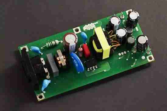
(power supply pcb)
In practical systems, DCDC converters and LDOs are often used together rather than as alternatives.
For example:
DCDC: 12V → 3.3V for efficient voltage conversion
LDO: 3.3V → 1.8V for noise-sensitive circuits such as ADCs, PLLs, and clocks
This approach combines the efficiency of a DCDC converter with the low-noise characteristics of an LDO, making it useful for applications that require both power efficiency and clean power rails.
Mistake 1: Insufficient Filtering at the LDO Input → Upstream Noise May Reach the Downstream Rail
Incorrect: Connecting the DCDC output directly to an LDO-powered sensitive load without evaluating the DCDC switching noise and the LDO's PSRR.
Consequence: Switching ripple from the upstream converter may couple into downstream sensitive circuits through the power path, affecting ADC, PLL, and other noise-sensitive devices.
Correct:
Mistake 2: Poor Power Region Layout → Noise Coupling
Incorrect: Placing the high-noise DCDC switching area too close to sensitive LDO power areas or creating unnecessary coupling between different power regions.
Consequence: Switching noise can couple into sensitive power rails through parasitic capacitance, electromagnetic coupling, or shared impedance.
Correct:
Mistake 3: Poorly Designed Decoupling Network → Insufficient High-Frequency Response
Incorrect: Placing all capacitors at the DCDC output while providing insufficient local decoupling near sensitive loads.
Consequence: Parasitic impedance in the power path can reduce high-frequency decoupling effectiveness, preventing the load from receiving transient current quickly enough.
Correct:
Although LDOs and DCDC converters are both power management devices, their power supply layout priorities are different.
LDO layout guidelines focus more on thermal management, capacitor placement, and power dissipation. DCDC PCB layout focuses more on high-frequency power loops, feedback paths, grounding, and EMI. Mixed power supplies require additional attention to noise isolation and decoupling between different power stages.
A good power supply pcb design is not simply about adding more copper. It is about giving current the shortest and most appropriate path, keeping noise away from sensitive areas, and placing every critical component where it can perform properly.