Mila
Jan 15,2026
7525
Mila
Jan 15,2026
7525
Differential Pair Routing Guidelines for High-Speed PCB Design
Overview of Differential Pair RoutingA differential pair consists of two coupled transmission lines. Differential signaling works by driving the pair with two complementary signals—one line carries th...
Mila
Jan 13,2026
3439
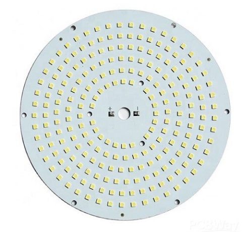
LED PCB Layout and Routing Guidelines: Practical Design Rules for Reliable Lighting
LED PCBs are not merely passive carriers; they are critical systems that determine the final performance, lifespan, and quality of a product. Their design directly impacts optical efficiency, reliabil...
Mila
Jan 09,2026
10755
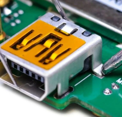
USB Type-C PCB Design Guidelines: Layout and Routing Best Practices
The USB interface has evolved through multiple generations and now reaches the era of USB 3.1 with 10 Gbps high-speed data transfer and up to 100 W power delivery. Among them, the Type-C connector has...
Mila
Jan 07,2026
3069
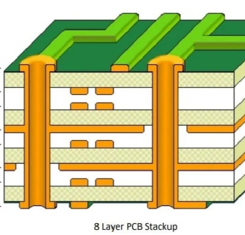
How to Select the Right HDI Stack-Up at the HDI Design Stage
Stack-Up Determines EverythingOnce the PCB stack-up is defined, nearly 80% of the total manufacturing cost is effectively locked in. This is especially true for HDI PCB design, where stack-up decision...

Mila
Dec 31,2025
3313
When to Choose Heavy Copper PCB: Standards, Performance, and Applications
Extra-long, extra-wide, ultra-thick, and heavy copper PCBs play a critical role in modern electronic devices. They are mainly used in high-power, high-current, harsh-environment, and space-constrained...
Mila
Dec 30,2025
4007
RF PCB Design Guidelines: Key Considerations for High-Frequency Circuits
In recent years, the rapid growth of Bluetooth devices, wireless local area networks (WLAN), and mobile communication systems has driven increasing attention to RF circuit design techniques. From past...
Mila
Dec 29,2025
12147
Payoneer Payment Instructions
To complete your payment via Payoneer, please follow the instructions below. Method 1: Payment Request(Recommended)With this method, PCBWay initiates an official payment request through Payoneer,...

PCBWay
Dec 26,2025
2331
PCBWay Store NewArrival Product - TS1M Multi-Function Mini Soldering Station
Link:TS1MThe TS1M Multi-Function Mini Soldering Station adopts a non-traditional design with a compact triangular body structure.Compatible with the PD 3.1 fast charging protocol (maximum 140W power);...
 Maykol Rey
Dec 23,2025
4218
Maykol Rey
Dec 23,2025
4218
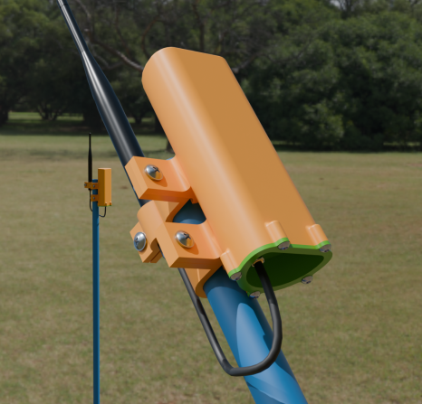
Standalone humidity sensor with LoRa
If you've already seen the Addon Battery YD-ESP32-S3 board I made to give autonomy to the YD ESP32 S3 development boards, you might be wondering: what could its application be?What could its applicati...
Mila
Dec 20,2025
5676
Flex PCB Bending Area Design Guidelines: How to Prevent Trace Cracking and Failure
Flexible circuit design involves many challenges. Flexible PCBs must overcome copper work hardening and fatigue, maintain adequate flexibility, and prevent tearing of the FPC substrate. In Flexible PC...
Mila
Dec 18,2025
4110
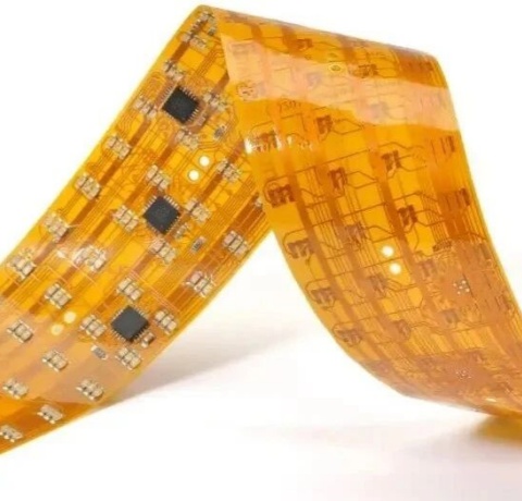
What Determines Flexible PCB Cost: Key Factors Explained
Flexible PCB (FPC), also known as a flexible circuit board, is a type of printed circuit board. However, it differs significantly from traditional rigid PCBs in structure and application, which is why...
Mila
Dec 12,2025
8540
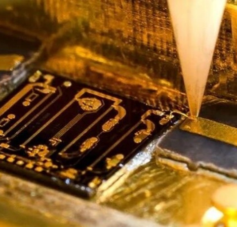
Gold Wire Bonding: Choosing the Right Gold Thickness and Surface Finish
Gold wire bonding is a PCB manufacturing process that uses extremely fine gold wires to connect the leads of a chip or device to PCB pads, electrodes, or lead frames. It is a wire bonding process that...
Mila
Dec 11,2025
4504
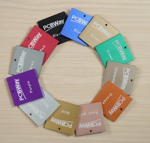
Anodized Aluminum Samples Showcase: Real Finishes, Colors, and Surface Quality
What is Anodized Aluminum?Aluminum anodizing is an electrochemical surface treatment process that converts the outer layer of aluminum into a durable, corrosion-resistant oxide layer. Unlike paint or ...

Mila
Dec 10,2025
4501
Design Tips to Prevent 3D Printing Failures and Reduce Support Waste
Failed prints and difficult support removal are among the most common sources of waste in 3D printing. They increase cost, reduce surface quality, and consume unnecessary time and material. Fortunatel...

 William Harter
Dec 06,2025
1844
William Harter
Dec 06,2025
1844
Tip for placing decoupling capictors
If you're using KiCad, here's a useful tip for organizing decoupling capacitors. In your schematic, assign references to each decoupling capacitor using the format C#-U#. For instance, if IC U1 has ca...
Mila
Dec 05,2025
7901
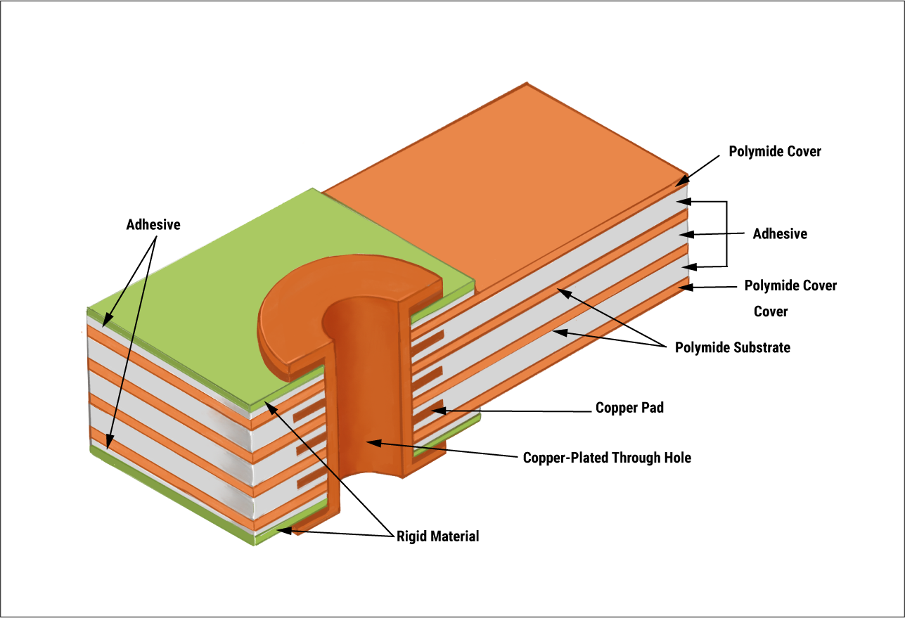
Rigid-Flex PCB Stack-Up
Rigid-Flex PCBs combine rigid circuit boards and flexible circuits into one integrated structure. They include robust rigid areas for component assembly and flexible areas that can bend or fold, with ...
Mila
Dec 03,2025
5439
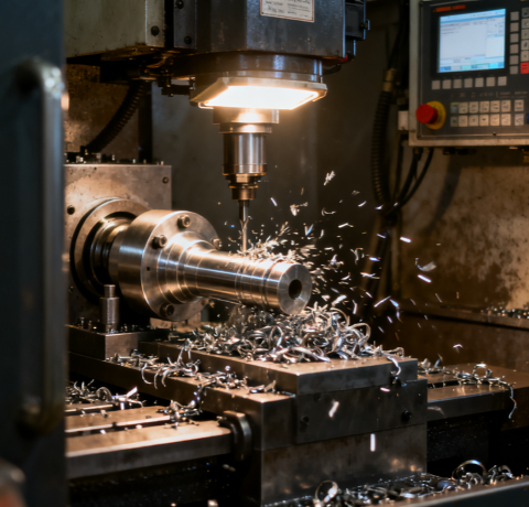
10 Ways to Reduce CNC Machining Costs: Practical Design Tips
CNC machining cost is mainly determined by machining time, material selection, setup time, and tool requirements. When a design includes special features such as very tight tolerances or ultra-thin wa...
William Harter
Dec 01,2025
2640
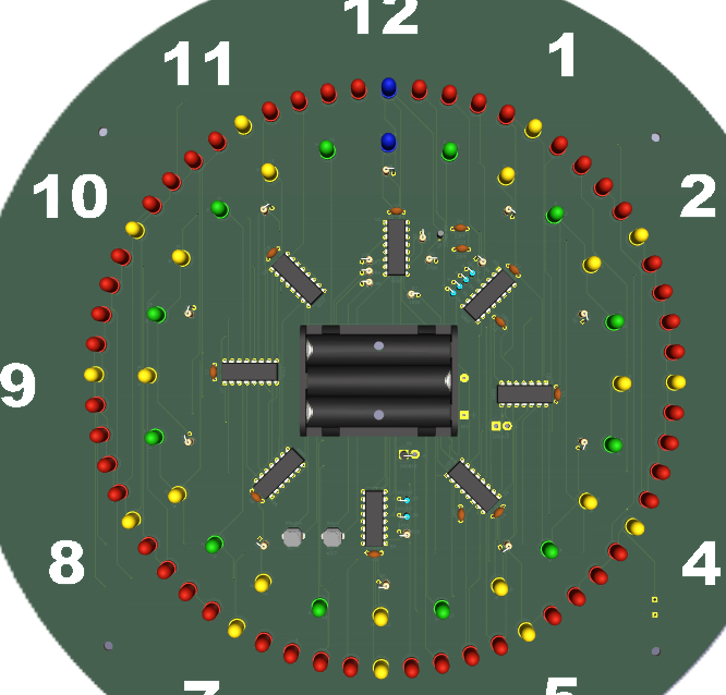
A desbription of my next share project.
My upcoming share project is a digital analog clock. The design uses a circle of 60 LEDs to indicate minutes and 24 LEDs to represent hours and half-hours. For the minutes, there are six groups of ten...
| Ranking | Name | Answers |
|---|---|---|
| 1 | PCBWay Team | 7 |