Unlike rigid PCBs, flexible PCBs (FPCs) can bend and fold to fit into compact electronic devices. They are widely used in smartphones, laptops, printers, and other products where space is limited or components need to move.
However, flexibility does not mean an FPC can bend without limits. Poorly designed bend areas can lead to copper trace cracks, delamination, or premature failure, especially in applications involving repeated bending. A reliable flex PCB design must account for bend radius, trace routing, copper foil selection, and stiffener placement.
In this guide, we’ll look at the key design considerations for FPC bend areas and how to improve their reliability in both static and dynamic bending applications.
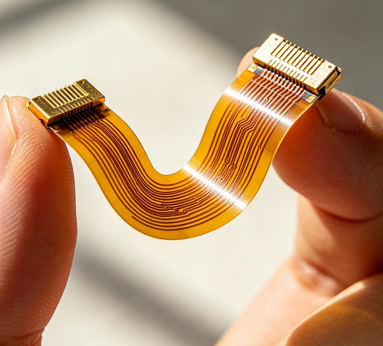
Vias are one of the key structures to watch when designing a flex PCB bend area. To simplify routing, inexperienced designers may place vias close to a bend line to change layers. However, repeated bending can eventually cause trace fractures and electrical failures.
The reason is straightforward: vias introduce structural transitions between the copper plating, pads, and substrate. Differences in material properties and geometry can affect local stress distribution. During repeated bending, stress may concentrate around the via, leading to copper fatigue and crack propagation over time. Eventually, the electrical connection may fail.
Design tip: Avoid placing through-holes, blind vias, or buried vias within the active bend area. If layer transitions are necessary, move the vias outside the bend area whenever possible. The required clearance depends on the bend geometry, board thickness, and manufacturer guidelines. A clearance of at least 1 mm can serve as an initial layout reference, but it is not a universal requirement for every FPC.
Resistors, capacitors, ICs, connectors, and other SMT components should generally not be placed in areas that undergo repeated bending.
Components are relatively rigid, while the flexible substrate deforms during bending. If a component sits within the bend area, additional mechanical stress may develop around its body, pads, and solder joints. Brittle components, such as ceramic capacitors, require particular attention because both solder joint cracking and component body damage are possible.
Design tip: Place components in rigid sections or reinforced areas, away from the actual bending region. A clearance of 2 mm beyond the bend boundary can serve as an initial reference, but the final distance should account for component size, stiffener geometry, and the actual bending range.
Trace direction affects how mechanical stress is distributed during bending. However, no single routing angle is best for every FPC structure.
When routing through a bend area, consider the actual bending axis, bending direction, and trace distribution. Avoid sharp corners, abrupt width changes, and locally crowded traces, as these features can create stress concentrations.
Traces perpendicular to the bending axis: This arrangement may be appropriate for traces crossing the bend area in certain single-axis bending structures, but it must be evaluated against the actual bending geometry.
Traces parallel to the bending axis: Whether this arrangement is suitable depends on the specific structure. It should not automatically be classified as the most failure-prone direction.
Traces at 45°: Angled routing may work in certain layouts, but its bending life cannot simply be assumed to fall between that of perpendicular and parallel traces.
For dynamic flex PCB applications, prioritize smooth, continuous traces, avoid sharp turns and abrupt geometry changes, and verify reliability through appropriate bending tests.
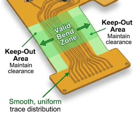
(flex PCB bend area design with via and component keepout zones)
When designing an FPC, some engineers focus mainly on whether it fits inside the enclosure. Reducing the bend radius too much may make assembly easier, but it can also shorten the product's service life.
First, distinguish between static and dynamic bending. Their design requirements are different.
Static bending: The FPC is bent during assembly and then remains in a relatively fixed position. Internal cables that do not move during normal operation are typical examples. A relatively small bend radius may be acceptable, provided it meets the requirements of the specific material and structure.
Dynamic bending: The FPC repeatedly bends during operation. Examples include foldable phone hinges, printer head cables, and robotic joints. These applications place greater demands on copper fatigue resistance, bend radius, and overall structural design.
For preliminary flex PCB design, the following values can serve as starting points:
These ratios are not universal standards. The actual requirement depends on factors such as single-sided or double-sided construction, copper layer count, copper foil type, material thickness, and the target number of bending cycles. For applications requiring a long flex life, follow the design guidelines provided by the material supplier or FPC manufacturer.
For example, if an FPC has a total thickness of 0.2 mm, the preliminary reference values would be:
These figures illustrate the calculation method only. They should not be treated as minimum design limits for every 0.2 mm FPC.
An excessively small bend radius can cause copper fatigue cracking, coverlay or substrate delamination, and, in severe cases, substrate damage. Any of these failures can eventually render the flexible circuit unusable.
Copper foil is an essential part of the FPC's conductive structure and a key factor in repeated-bending reliability. When choosing copper foil, consider whether the application involves static or dynamic bending rather than focusing on cost alone.
Electrodeposited copper (ED copper): ED copper is produced through an electrodeposition process and offers mature manufacturing processes and cost advantages. Its grain structure differs from that of rolled copper, and its fatigue performance should be evaluated carefully for repeated-bending applications. For applications involving relatively few bending cycles, ED copper may be considered depending on the specific design and manufacturer recommendations.
Rolled-annealed copper (RA copper): RA copper is produced through rolling and annealing. It generally offers good ductility and flexing performance, making it suitable for FPCs that require a longer dynamic flex life. Although it typically costs more, it may help improve reliability in applications involving repeated bending.
The key takeaway is simple: For static applications, select copper foil based on cost and performance requirements. For dynamic applications with high cycle counts, RA copper is generally the preferred starting point, subject to verification of the bend radius, copper thickness, and target service life.
In addition to the major design restrictions discussed above, several details deserve attention during flex PCB routing and layout.
Trace direction: Determine the routing direction based on the actual bending axis and motion. Traces should remain smooth and continuous, with unnecessary sharp turns avoided.
Trace width and spacing: Choose appropriate trace widths and spacing to meet electrical and manufacturing requirements. Distribute multiple traces evenly across the bend area instead of crowding them into one section. The final dimensions should account for the bending structure, copper thickness, and manufacturing capabilities rather than relying on a fixed width-to-spacing ratio.
Corners and width transitions: Use rounded corners or smooth transitions wherever practical. Avoid sharp corners and abrupt changes in trace width to reduce stress concentrations. Minimize unnecessary crossovers and layer transitions within the bend area.
Coverlay: Flexible coverlay is commonly used to protect copper traces in bend areas and reduce the risk of wear and oxidation. Position coverlay openings carefully, keeping coverlay edges away from regions of high mechanical stress. Confirm the required coverage and manufacturing details for the specific design.
Stiffeners increase local rigidity in an FPC. They are commonly used beneath connectors, gold fingers, and SMT components. However, stiffeners should not extend into the active bend area where the FPC needs to flex freely.
Stainless steel stiffeners: Stainless steel provides relatively high rigidity and is commonly available in thicknesses of approximately 0.1–0.3 mm. It is often used behind connectors and gold fingers to improve structural support and withstand insertion and removal forces. Pay attention to edge geometry and transitions to prevent sharp edges from damaging the FPC substrate.
PI stiffeners: Polyimide (PI) stiffeners are generally thinner and more flexible than metal stiffeners. They can be used beneath certain SMT components or in areas that require localized reinforcement while retaining some flexibility. Their actual rigidity depends on the material thickness and structure. Stress concentrations near stiffener edges should also be considered.
Regardless of the stiffener type, keep it outside the active bend area. The required clearance depends on the bending range, stiffener thickness, and overall structure. A fixed 2 mm clearance alone cannot guarantee a reliable design.
Design factorStatic bendingDynamic bendingBend radiusApproximately 6× board thickness as an initial reference; verify the designApproximately 10× board thickness or greater as an initial reference; verify the designCopper foilSelect according to cost and performanceRA copper is generally preferred for high-cycle applicationsLayer countSelect according to electrical and mechanical requirementsMinimize layer count where practical; single- or double-sided designs are often preferredTrace directionDetermine based on the bending geometryDetermine based on the actual motion and bending axisVias and componentsAvoid within the active bend areaAvoid within the active bend areaCoverlayDesign according to structural and protection requirementsPay particular attention to coverlay edges and repeated-bending reliabilityStiffenersPlace outside the active bend areaKeep outside the active bend area and manage edge-related stressTypical applicationsFPCs bent during assembly and then fixed in placeFoldable phones, printer head cables, robotic joints, and other moving assemblies
Before submitting your FPC design files, use the following checklist to review the bend area:
Ultimately, successful flex PCB design comes down to controlling bending strain, minimizing local stress concentrations, and ensuring that the materials and structure meet the required flex life. Keep vias and components out of active bend areas, route traces smoothly, allow sufficient bend radius, and select copper foil carefully for dynamic applications. For products that undergo repeated bending, validate the design through testing rather than relying on general rules of thumb alone.



