 Mila
Jun 18,2026
1448
Mila
Jun 18,2026
1448
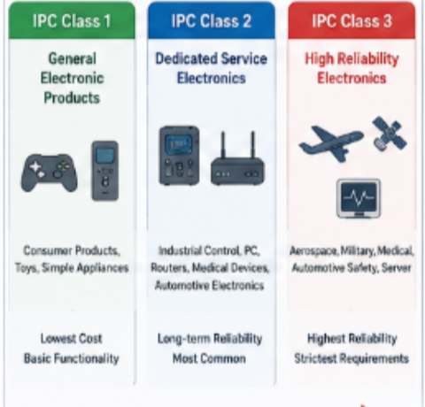
Designing Production-Ready PCBs with IPC Standards
IPC standards are the foundation of modern PCB design, manufacturing, and assembly. By providing a unified set of technical requirements, they help engineers improve reliability, manufacturability, an...
Mila
Jun 17,2026
1138
PCB Annular Ring Design: Sizing, IPC Standards, DFM Rules, and Failure Prevention
In PCB design, the annular ring may seem like a small feature, but it directly affects electrical reliability, solder joint strength, and manufacturing yield. Insufficient annular ring width can lead ...
Mila
Jun 12,2026
1829
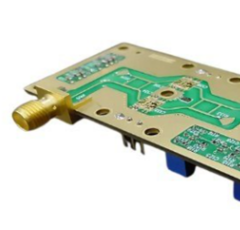
RF PCB Design Guide: Layout, Stackup, Routing and Manufacturing Best Practices
RF PCB design is significantly more challenging than conventional PCB design due to the effects of high-frequency signal propagation, impedance discontinuities, and electromagnetic interference. Even ...
 William Harter
Jun 12,2026
470
William Harter
Jun 12,2026
470
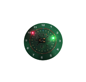
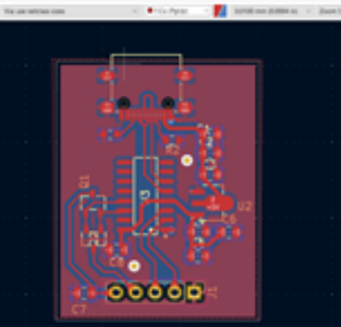
My current shared project LED Ring Clock
My shared clock project is now available on PCBWay. This is the second version of my LED ring clock, which uses two LED rings: the inner ring shows the hours and half hours, and the outer ring shows t...
Mila
Jun 09,2026
740
Circuit Symbols Explained: A Complete Guide to Electronic Symbols and Schematic Symbols in PCB Design
In electronic product development, hardware design, equipment maintenance, and PCB design, schematic diagrams serve as the essential bridge between design, manufacturing, and debugging. At the core of...
Mila
Jun 04,2026
1161
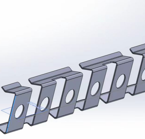
Sheet Metal Bending Design Guide: DFM Rules, Bend Radius, Bend Allowance, and Manufacturing Best Practices
Although sheet metal bending appears to be a simple manufacturing process, many production issues—including cracking, hole distortion, tooling interference, excessive springback, and assembly failures...
PCBWay
Jun 03,2026
1592
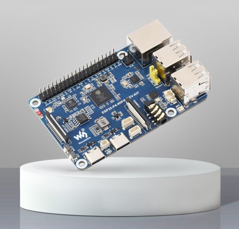
PCBWay Store NewArrival Product - ESP32-P4-WIFI6-DEV-KIT High-Performance Development Board
Link:ESP32-P4-WIFI6-DEV-KITESP32-P4-WIFI6-DEV-KITDevelopment BoardHigh-performance Development Board Based On ESP32-P4 And ESP32-C6Rich Human-machine Interfaces Development Board IntroductionThis...
Mila
May 28,2026
1037
Sheet Metal Box Design Guide: 12 Common DFM Mistakes to Avoid
Sheet metal fabrication is widely used for enclosures, brackets, chassis, and industrial housings through processes such as cutting, bending, welding, and surface finishing. Although many designs look...
Mila
May 26,2026
2074
Complete Sheet Metal Box Design Guide for Electronic Enclosures
With the advantages of controllable cost, reliable strength, and efficient manufacturing, sheet metal enclosures are widely used in electronics, industrial control, telecommunications, medical equipme...
 Engineer
May 22,2026
1434
Engineer
May 22,2026
1434
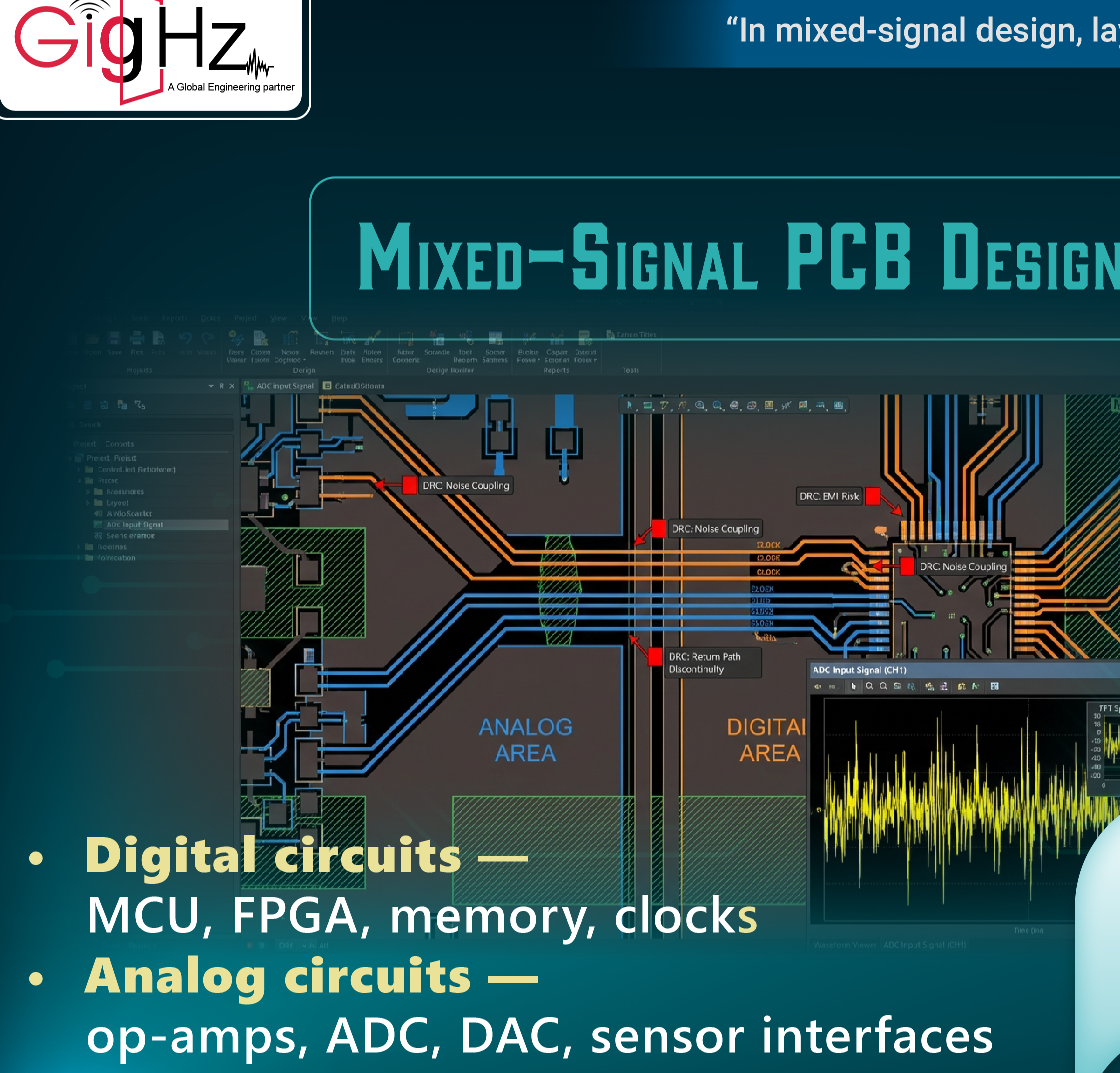
Mixed-Signal PCB Design: A Practical Engineering Guide
Mixed-Signal PCB Design: A Practical Engineering GuideMany PCB performance issues are not caused by firmware or components — they originate in the layout itself.When a mixed-signal board shows unstabl...
Mila
May 21,2026
3092
Decoupling Capacitor Placement Guidelines for High-Speed PCB Design
Many high-speed PCBs appear correct during schematic design, yet after fabrication, problems such as FPGA configuration failures, unstable DDR timing, ADC noise, EMC radiation issues, and excessive po...
Mila
May 18,2026
2770
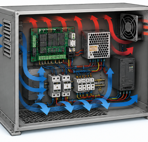
Electronic Enclosure Thermal Management: Cooling Design and Best Practices
Enclosure thermal management is critical for preventing overheating, condensation, and premature electronic component failure. A well-designed enclosure cooling system helps maintain stable operating ...
Mila
May 14,2026
3433
EMI Shielded Enclosure Design Guide: Principles, Materials, and Best Practices
EMI (Electromagnetic Interference) has become a major challenge in modern electronic systems. In many projects, EMI-related issues do not appear during early development, but instead emerge during EMC...
Mila
May 11,2026
3358
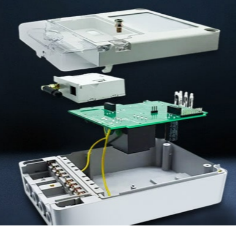
PCB Enclosure Design Guide: Materials, IP Ratings, and Structural Best Practices
In electronic product development, enclosure design is often underestimated. Even when the PCB functions correctly, poor enclosure design can still lead to overheating, assembly interference, insuffic...
Mila
May 07,2026
1807
Basic PCB Design: Complete PCB Design Guidelines for Beginners
PCB is the core carrier of modern electronic devices. From wearable products to servers and automotive electronics, reliable PCB design is essential to system performance and stability. Many beginners...
Mila
Apr 30,2026
1543
DCDC Power PCB Layout Guidelines: Reduce Noise, Improve Stability, and Pass EMC
In DCDC power design, the circuit defines the function, but PCB layout determines success or failure. Even with correct component selection and accurate calculations, issues such as audible noise, ove...
| Ranking | Name | Answers |
|---|---|---|
| 1 | PCBWay Team | 7 |