
 Anson
Mar 01,2023
9852
Anson
Mar 01,2023
9852
5A-35V Adjustable Switching Power Supply
By Hesam Moshiri, Anson BaoCopyright: Attribution-NonCommercial-NoDerivs (CC-BY-NC-ND)A DC-to-DC converter is one of the most commonly used circuits in electronics, especially in power supply applicat...

 Mia
Feb 27,2023
7451
Mia
Feb 27,2023
7451
Why is PCB Production Compensation Necessary
During the design and manufacturing process of PCB, there may be some factors such as material properties, manufacturing processes, environmental factors, etc., which may cause changes in the electric...

PCBWay
Feb 27,2023
30830
Via-in-Pad Design | PCB Knowledge
What is a Via-in-Pad?As electronic products become increasingly miniaturized, multi-functional, and highly integrated, PCBs need to accommodate higher routing densities. To meet this demand, via-in-pa...
PCBWay
Feb 23,2023
48695
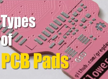
Types of PCB Pads | PCB Knowledge
What is a PCB Pad?A pad is the exposed area of copper on a circuit board, where the component lead is soldered. The electrical connection of all components is made via pads. The design and placement o...

PCBWay
Feb 13,2023
75575
What is a PCB Via? | PCB Knowledge
In multi-layer PCB design and manufacturing process, the term “via” is extensively used. However, what does the via mean, and how to use it in designs? In this video, we’ll cover some basics about the...
Anson
Feb 02,2023
15737
30A AC Soft Starter (Inrush Current Limiter)
By Hesam Moshiri, Anson BaoCopyright: Attribution-NonCommercial-NoDerivs (CC-BY-NC-ND)Are you tired of dealing with the damaging effects of inrush currents on your industrial devices? Look no further ...

 Engineer
Jan 23,2023
3402
Engineer
Jan 23,2023
3402
Basic Things For Generating High-Speed Printed Circuit Board
As the world is upgrading at a very fast rate, every field is producing a faster product which is the reason for embedded software development. Speed is inversely proportional to the size in terms of ...

PCBWay
Jan 13,2023
10256
How to Place PCBWay Orders from Online 3D Viewer Directly?
Online 3D Viewer (https://3dviewer.net/) is popular among 3D Printing hobbyists for its simple page and excellent viewing capabilities. For the convenience of all, we have good news: PCBWay has partne...

PCBWay
Jan 11,2023
18203
How to Generate BOM and Centroid File in Eagle
In Eagle, we usually find that the file format is often confusing when using the normal way to export BOM and Centroid files. To solve the problem, this article will introduce how to export correctly ...

PCBWay
Jan 03,2023
12175
CNC Ordering Process | PCBWay Website Exploration 07
Welcome back to the PCBWay website exploration. In addition to PCB manufacturing services, PCBWay also offers CNC Machining, 3D Printing, Sheet Metal Fabrication, Injection Molding, and Vacuum Casting...

Anson
Dec 30,2022
12465
Wireless Home Automation (Control and Monitoring) Using a Nextion HMI Display
By Hesam Moshiri, Anson BaoCopyright: Attribution-NonCommercial-NoDerivs (CC BY-NC-ND)Nowadays home automation is a trending topic among electronic enthusiasts and even the mass population. People are...

PCBWay
Dec 23,2022
9518
Module Store | PCBWay+ Community | PCBWay Website Exploration 06
The module store is another popular part of our community, and it provides you with popular modules and special PCBWay gadgets. For all the listed products in our store, you can directly buy them in c...

PCBWay
Dec 16,2022
7224
Post-processing of 3D Printing
After 3D printing is complete, the part usually needs to be post-processed. Post-processing refers to all the work performed after the part comes out of the 3D printer, and this piece of&nbs...

PCBWay
Dec 16,2022
4151
Hamster Mix
Hamster Mix is a MIDI controller based on Arduino, with a function to be connected by bluetooth. By using it,you are able to play MIDI notes within five octaves.It has twelve keys and the ability to s...

PCBWay
Dec 12,2022
15681
Shared Projects | PCBWay+ Community | PCBWay Website Exploration 05
The PCBWay+ community is a platform for electronics enthusiasts and makers to share projects, discuss topics in electronics, find information about PCB design, and get help for projects. This communit...
PCBWay
Dec 09,2022
13120
How to Generate Gerber in Cadence Allegro
1. Check the PCB status, and make sure that the displayed results are all green.2. Double-check for Database Check.3. Gerber output settings.4. Generate Drill file:Click [ Manufacture->NC->NC Dr...

PCBWay
Dec 08,2022
12468
Introduction of 3D Printing Wall Thickness
Wall thickness refers to the distance between a surface to its corresponding surface. Generally speaking, the thicker the wall thickness of 3D printing, the greater the hardness and strength of the pa...
| Ranking | Name | Answers |
|---|---|---|
| 1 | PCBWay Team | 3 |
| 2 | Engineer | 1 |
| 3 | sheng wang | 1 |
| 4 | olDirdey | 1 |


