In multi-layer PCB design and manufacturing process, the term “via” is extensively used. However, what does the via mean, and how to use it in designs? In this video, we’ll cover some basics about the PCB via.
A via is a small drilled hole that goes through two or more adjacent layers. It allows the signals and power to travel between layers. As the circuits between the layers of a multilayer PCB are independent of each other, vias are important means to establish inter-layer connections. Depending upon their functionality, vias are commonly classified into three types—blind via, buried via, and through-hole via.
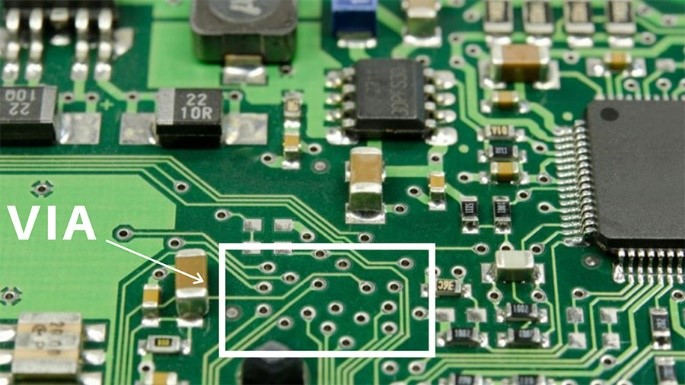
Figure1. What is a Via
Blind via: (From outer layer to inner layer)
A blind via extends from one side of the outer layer, (either the top or bottom layer) and connects at least one inner layer, but does not pass through the entire board. Therefore, blind vias are exposed only on one side of the board. In PCB design, blind vias can help free up some extra space and are commonly used in BGA assembly and HDI PCBs.
Buried via: (From inner layer to inner layer)
A buried via connects at least two inner layers and it’s not visible on the outer layer. It is designed mainly to connect inner layer signals, which can reduce the chance of signal interference, so are suitable for HDI PCBs.
Through-hole via: (From outer layer to outer layer)
The through-hole via is the most common type of via in PCB manufacturing, which connects the inner and outer layers and passes through the entire board. It is usually used for internal interconnection of the board or as a mounting hole for components.
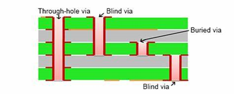
Figure2. Types of Vias
There are three main methods for via covering processes: tenting vias, vias not covered, and plugged vias with solder mask.

Figure3. Via Covering Process
Tenting vias
Tenting vias is the process to cover the annular ring of the via with solder mask to achieve insulation. It is important to ensure that the annular ring is fully covered with the solder mask and the solder mask is thick enough to avoid accidental short circuits or contact with the circuit.

Figure4. Tenting vias
Vias not covered
When you choose the “vias not covered” for your PCB design, it means both the via hole and the annular ring will not be covered with solder mask. These uncovered vias are usually used to debug measurement signals. Also, leaving vias uncovered has other advantages. For example, it can increase the heat dissipation area, which is conducive to heat dissipation. Therefore, if you have high requirements for board heat dissipation, you can choose this process. The problem with this process is that it is easy to cause a short circuit.

Figure5. Vias not covered
Plugged vias with solder mask
Vias plugged with solder mask is the process to prevent the solder ball from popping out to cause a short circuit during wave soldering, and avoid flux residue in the via hole. Generally, if the board has a BGA or IC assembly, it is necessary to select the mask-plugged vias.
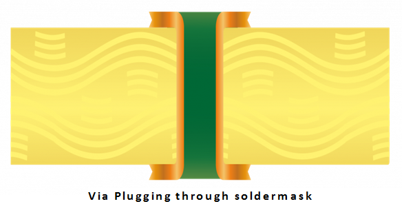
Figure6. Vias plugged with solder mask
Unlike through-hole vias, blind and buried vias are only available on boards with at least four layers. The use of blind or buried holes is an effective way to increase the density of multilayer boards, and reduce the number of layers and board dimensions. However, in comparison, through-hole via is easy and cheaper to manufacture, so in PCB designs they are more commonly used.


